
NVIDIA Officially Launches GeForce GTX 650 GPU (Updated!)
NVIDIA has officially launch the GeForce GTX 650 GPU. It features the full implementation of a Kepler GK107 chip, with 384 CUDA cores, clocked at 1058MHz. We first reported on its possible launch in August this year and it appears that most of the technical details leaked are accurate.

NVIDIA has officially launch the GeForce GTX 650 GPU. It features the full implementation of a Kepler GK107 chip, with 384 CUDA cores, clocked at 1058MHz. We first reported on its possible launch, together with the GeForce GTX 660, in early August this year. It appears that most of the technical details leaked in the early report are accurate. The GK107 chip has been first employed in the GT 640 range and is considered to be an entry-level Kepler class product. As such, the GTX 650 utilizing the same core is just a speedier edition to maximize the better manufacturing yields from TSMC's fabrication plants.

(Image Source: NVIDIA)
Model | GeForce GTX 650 | GeForce GT 640 |
Core Code | GK107 | GK107 |
Transistor Count | 1300 million | 1300 million |
Manufacturing Process | 28nm | 28nm |
Core Clock | 1058MHz | 950MHz |
Stream Processors | 384 Stream processing units | 384 Stream processing units |
Stream Processor Clock | 1058MHz | 950MHz |
Texture Mapping Units (TMU) or Texture Filtering (TF) units | 32 | 32 |
Raster Operator units (ROP) | 16 | 16 |
Video Memory Size | 1 / 2GB GDDR5 | 1 / 2GB GDDR5 |
Memory Clock | 5000MHz GDDR5 | 5000MHz GDDR5 |
DDR Memory Bus | 128-bit | 128-bit |
Memory Bandwidth | 80GB/s | 80GB/s |
PCI Express Interface | PCIe ver 3.0 x16 | PCIe ver 3.0 x16 |
Molex Power Connectors | 1 x 6-pin (TDP: 64W) | Nil (TDP: 75W) |
Video Connectors | 2 x DL-DVI, 1 x mini-HDMI | 2 x DL-DVI, 1 x mini-HDMI |
Of course the main star for today's big launch is the GeForce GTX 660 with a true performance mid-range GPU (GK106). While the processing prowess differs greatly, the main feature difference of the GTX 650 when compared to the GTX 660 is the former's lack of support for GPU Boost; however, NVIDIA says that cards based on the GeForce GTX 650 will have overheads for overclocking performance. The reference card NVIDIA GeForce GTX 650 will ship with a 6-pin Molex power connector that more than suffices for its stated power requirements. The company mentions that they expect their add-in partners to launch a slew of overclocked GTX 650 cards to target value-conscious consumers. The suggested SRP for the GeForce GTX 650 is US$109 and it is targeted squarely at the AMD Radeon HD 7750 graphics cards.
(Source: NVIDIA)
Basic Specifications | |
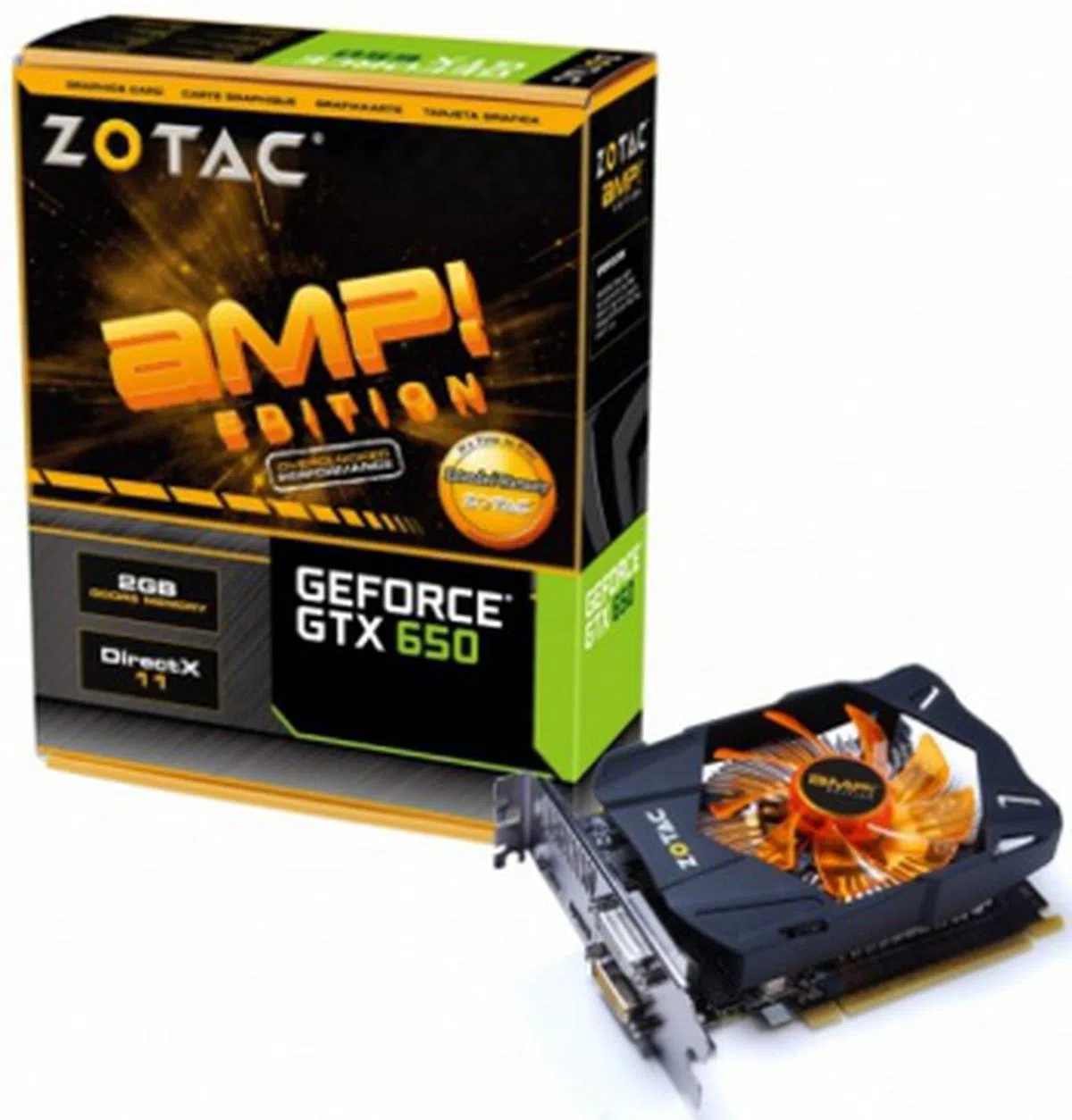
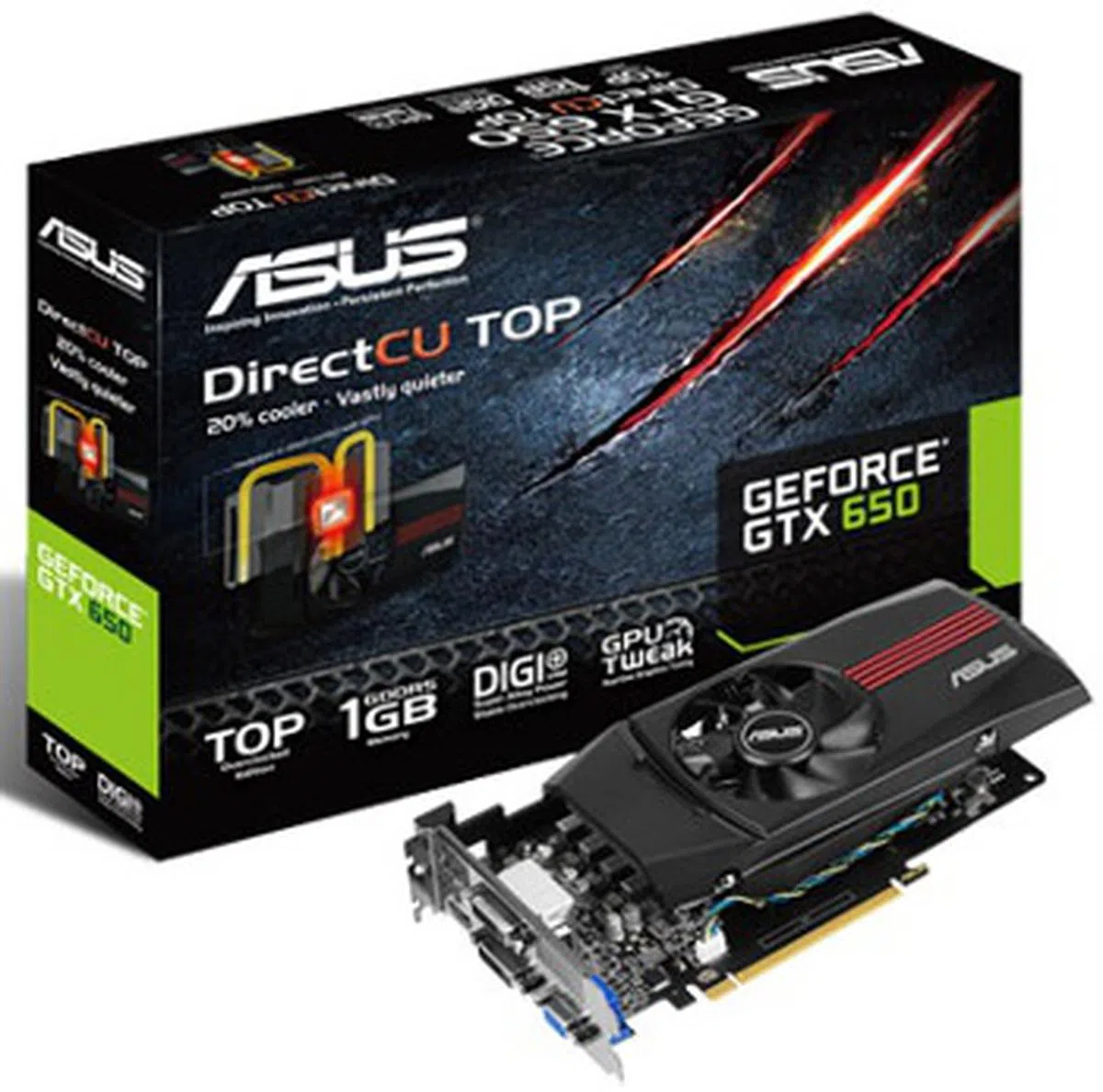 | Core Clock: 1215MHz Memory Clock: 5100MHz CustomCooler: DirectCU |
 | Core Clock: 1058MHz
Memory Clock: 5000MHz Custom Cooler: DirectCU |
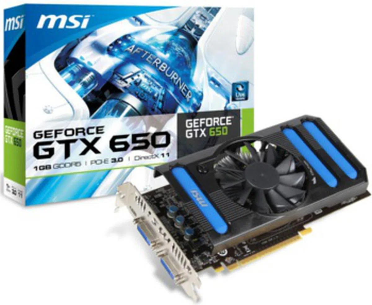
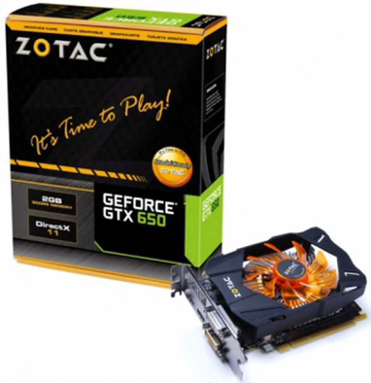
(in 1GBand 2GBversions) Core Clock: 1202MHz Memory Clock: 5000MHz | |
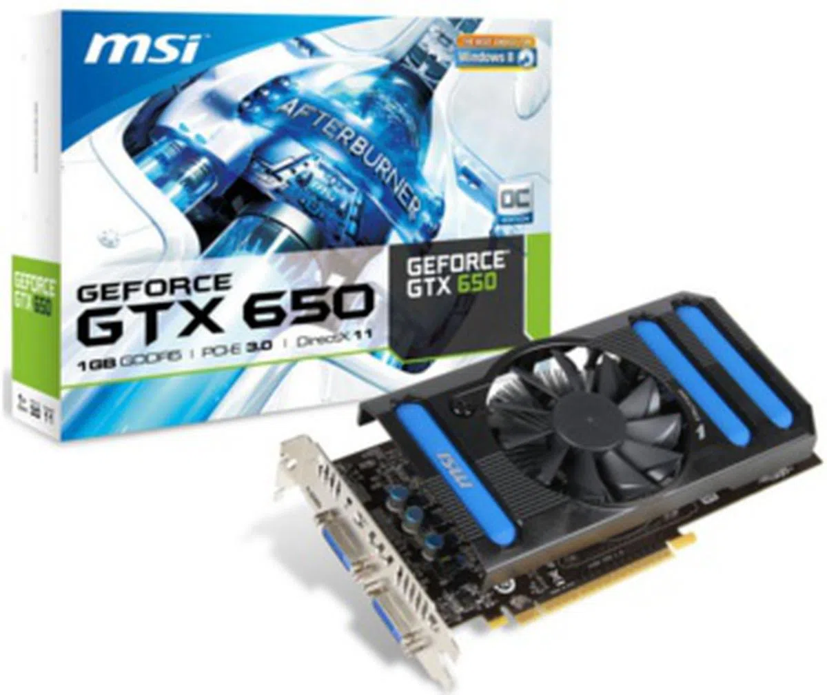
 | (in 1GBand 2GBversions) Core Clock: 1058MHz Memory Clock: 5000MHz |
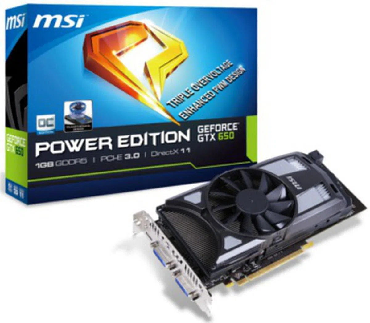
 | Core Clock:1058MHz
Memory Clock: 5000MHz Custom Cooler: Propeller Blade Technology |
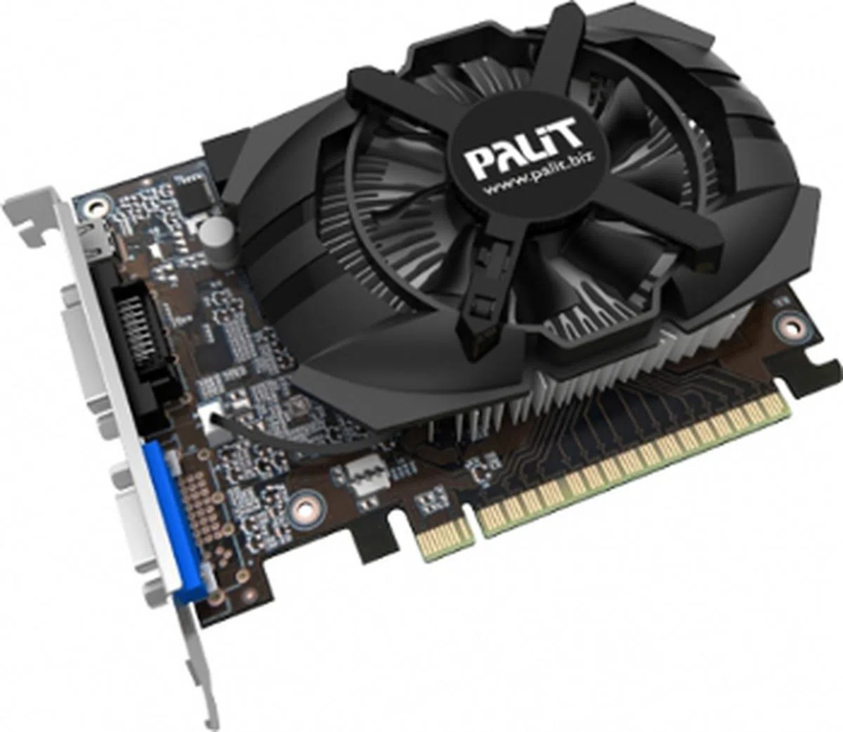
 | Core Clock: 1084MHz
Memory Clock: 5000MHz Custom Cooler: Propeller Blade Technology |
| Core Clock:1058MHz
Memory Clock: 5000MHz Custom Cooler: TwinThermal with Dust Removal technology |
 | Core Clock: 1124MHz
Memory Clock: 5000MHz Custom Cooler: TwinThermal with Dust Removal technology |
 | (3 versions) Core Clock: 1058MHz (1071MHz for the OCedition) Memory Clock: 5000MHz (5200MHz for the OCedition) |
Core Clock:1098MHz
Memory Clock: 5000MHz Custom Cooler: Dragon Cyclone (single specialized fan) | |
Core Clock: 1124MHz
Memory Clock: 5600MHz Custom Cooler:Dragon Cyclone (3 specialized fans) | |
 | (in 1GBand 2GBversions) Core Clock: 1071MHz Memory Clock: 5000MHz |
 | Core Clock: 1189MHz
Memory Clock: 5600MHz |


Our articles may contain affiliate links. If you buy through these links, we may earn a small commission.