
NVIDIA’s 80-billion transistor H100 GPU and new Hopper Architecture will drive the world’s AI Infrastructure
6 breakthrough areas define the new Hopper Architecture and the H100 super chip, so find out what they are and the whole convoy of H100-based solutions.

Note: This article was first published on 23rd March 2022 and updated with more details on 4th April 2022.
Meet the NVIDIA H100 GPU, NVIDIA's new battle unit of the era of accelerated AI computing with 80 billion transistors at its core.
Three years have passed since NVIDIA's Ampere architecture based A100, a GPU that kick-started the data centre revolution. Today, at GTC 2022, NVIDIA CEO Jensen Huang acknowledged the importance of advancing AI and, to that extent, launched a new processing engine to manage the world's AI infrastructure through its next-generation accelerated computing platform with the NVIDIA Hopper architecture.
Named after Grace Hopper, a pioneering computer scientist, the NVIDIA Hopper architecture will supersede the already powerful NVIDIA Ampere architecture. The all-new NVIDIA H100 is the company's first Hopper-based GPU that packs a whopping 80 billion transistors. This monster of a GPU boasts AI training performance throughputs up to 9x faster than the predecessor NVIDIA A100, 30 times more throughput for AI inferencing performance and up to seven times more HPC performance. As powerful as the NVIDIA A100 is, this level of performance leap over it is phenomenal, to say the least.
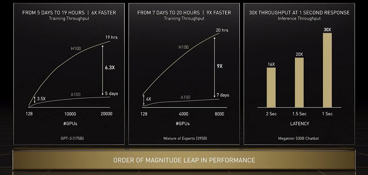
Performance leap of H100 vs. A100. Click to view a larger image.
It goes without saying that the NVIDIA H100 sets a new standard in accelerated large-scale AI and HPC capabilities, and this is made possible via these seven innovation breakthroughs:-
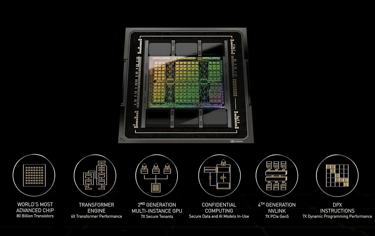
1) World's most advanced chip

(Click to view a larger image.)
Built with 80 billion transistors using a cutting-edge TSMC 4N process designed for NVIDIA's accelerated compute needs, H100 features significant advances to accelerate AI, HPC, memory bandwidth, interconnect and communication, including nearly 5TB per second of external connectivity. H100 is the first GPU to support PCIe Gen5 and the first to utilise HBM3, thus doubling the memory bandwidth to a staggering 3TB/s. Even the L2 cache has been bumped up to 50MB (previously 40MB) to better fit more significant portions of datasets and models, thus reducing HBM3 memory access.
To put that into perspective, NVIDIA says just twenty H100 GPUs can sustain the equivalent of the entire world's internet traffic, making it possible for customers to deliver advanced recommender systems and large language models running inference on data in real-time. Here's how the brand new H100 compares against its predecessors:-
Graphics Card | H100 (SXM) | A100(SXM) | Tesla V100 |
GPU | Hopper
(GH100) | Ampere
(GA100) | Volta
(GV100) |
Process | 4N
(TSMC) | 7nm
FinFET(TSMC) | 12nm FinFET |
Die Size (mm2) | 814 | 826 | 815 |
Transistors | 80 billion | 54 billion | 21.1 billion |
Streaming Multiprocessors (SM) | 132 | 108 | 80 |
CUDA cores (FP32) | 16896 | 6912 | 5120 |
Tensor Cores | 528 | 432 | 640 |
Tensor Performance1 (FP32) | 500 - 1000 TFLOPS | 156 - 312 TFLOPS | 120 TFLOPS |
RT Cores2 | NIL | NIL | NIL |
GPU boost clock speeds3 | TBD | 1410MHz | 1455MHz |
GPU Memory | 80GBHBM3 | 40GB HBM2 | 16GB HBM2 |
Memory clock speed | TBD | 2.4Gbps | 1.75Gbps |
Memory bus width | 5120-bit | 5120-bit | 4096-bit |
Memory bandwidth | 3TB/s | 1.6TB/s | 900GB/s |
Interconnect | 4th-gen NVLink(900GB/s)
+ PCIe 5.0 | 3rd-gen NVLink(600GB/s)
+ PCIe4.0 | 2nd-gen NVLink(300GB/s)
+PCIe3.0 |
Multi-Instance GPU (MIG) support | 7 MIGs with confidential compute | 7 MIGs | -- |
GPU board form factor | SXM5 | SXM4 | SXM2 |
TDP | 700W | 400W | 300W |
Price | -- | -- | -- |
1. Effective Tensor performance with and without using the Sparsity feature.
2. Data Center GPUs do not have RT Cores for ray-tracing, media encoder and display connectors as these GPUs are meant for installation in servers and data center racks to power AI and HPC tasks.
3. GPU peak and boost clocks are synonymous in NVIDIA Data Centre GPUs. Not yet finalised for H100.

2) Fourth-Gen Tensor Cores and updated Streaming Multiprocessor (SM) offer massive speed-up
With a new fabrication process, NVIDIA bumped up the number of streaming multiprocessors (SM) it can pack and boosted its clocks considerably over the A100. This has massively helped improve the H100's fourth-generation Tensor Core's performance by at least three times the throughput of the A100.

Those are some impressive stats for the new Hopper H100 chip.
To recap, the Tensor Core is a crucial piece to advance math operations for Matrix Multiplication and Accumulation (MMA) to deliver next-gen performance for HPC and AI tasks compared to traditional FP, INT and fused multiple accumulation (FMA) operations that are part of the main SM's pipeline.
The fourth-gen Tensor Core also adds a new FP8 data format, which halves the data storage and doubles the throughput compared to a traditional FP16 data type. With an updated compiler to take advantage of the new data format, the H100 can theoretically speed-up crunching FP16 data types through the FP8 format more than six times faster (inclusive of architectural advancements) than the A100 can on its own in FP16 format. That's under the assumption that the data that needs to be processed can do with less precision and still maintain the required accuracy, a trait that's further aided by the new Transformer Engine (more on this later).
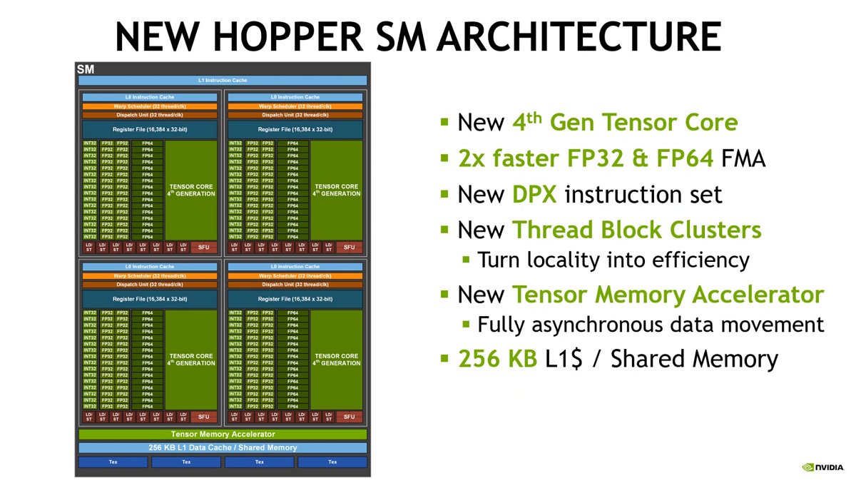
A brief look at the updated Hopper Streaming Multiprocessor. (Click to view a larger image.)
The new Tensor Core also boasts far more efficient data management, which saves up to 30% operand delivery power. This is thanks to Distributed Shared Memory, which enables more efficient communications directly between SM-to-SM using shared memory blocks within the same cluster. This offers a 7x reduction in latency to access different SM units on the H100 than writing to global memory on the A100 before other SM blocks can use the data. Yet another proponent that adds to more efficient data management is improvements in asynchronous execution via a new Asynchronous Transaction Barrier to improve data exchange or memory copy functions, as well as Tensor Memory Accelerator (TMA), which is essentially what DMA does for memory but specific to the usage of tensor cores.
3) New Transformer Engine
Transformers are deep learning models that have unlocked serf-supervised learning in a big way in the fields of natural language processing (NLP) for translations and text summaries, as well as computer vision (CV). Google's BERT is an early example of a Transformer machine learning model that has been widely used. Head over to this Wikipedia page for more base knowledge on Transformer deep learning model.

The rise of the Transformers. (Click to view a larger image.)
As AI progressed through various stages of development from just image classification, to recommendation engines, language translation modelling, and, more recently, the ability to produce conversational AI and avatars such as in Omniverse Avatars, many of the later developments were traced back to the Transformer deep learning model. NVIDIA also states that 70% of academic AI papers submitted in the last couple of years were based on Transformer models.
Increasingly, Transformers have become the cornerstone of AI evolution, and NVIDIA believes the next wave of AI will be further fuelled by Transformers. This is why the new Hopper architecture and H100 chip features a brand new Transformer Engine to speed up these neural networks by as much as six times the previous generation GPU without losing precision or accuracy.
Transformer model training can be reduced from weeks to days – NVIDIA CEO, Jensen Huang.
The new Transformer Engine uses software and custom NVIDIA Hopper Tensor Core technology to accelerate training and inference of transformer models, the prevalent AI model building block. These Tensor Cores can now apply mixed FP8 and FP16 formats dynamically and intelligently without performance or accuracy loss to dramatically increase AI calculation for transformers. It will also automatically handle re-casting and scaling between these precisions in each layer.
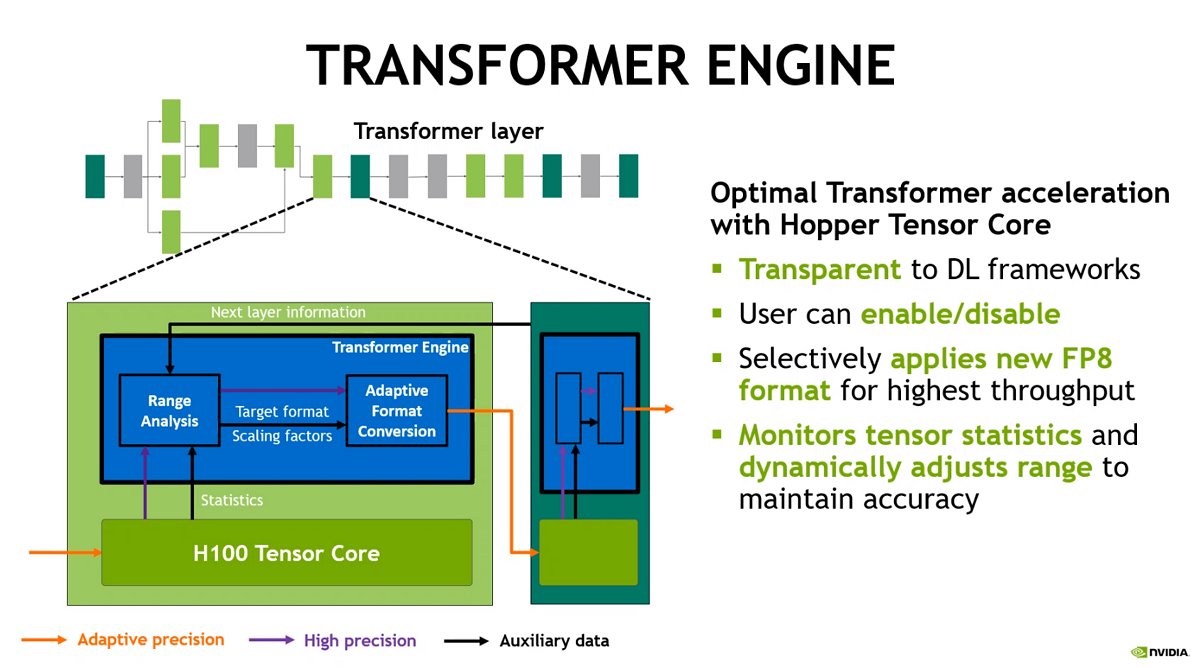
Dynamic mixed-precision processing is a key feature of the new Transformer Engine that's part of the 4th-gen Tensor Core of the Hopper architecture. (Click to view a larger image.)
As iterated earlier, the Hopper architecture's new fourth-gen Tensor Cores triple floating-point ops. When combined with the new Transformer Engine and fourth-gen NVLinks (covered more in a later point), the Hopper Tensor Cores enable an order-of-magnitude speed-up for HPC and AI workloads.
4) Second-gen Secure Multi-Instance GPU (MIG)

For cloud computing, multi-tenant infrastructure translates directly to revenues and cost of service.
The Ampere A100 was the first to sport Multi-Instance (MIG) functionality to partition the GPU into seven independent instances or seven virtual GPUs, each with its own resources (memory, cache, streaming multiprocessors) to tackle various workloads. The new Hopper H100 extends MIG capabilities that's 7x the previous generation by offering secure multi-tenant configurations in the cloud across each GPU instance. The A100 was only able to do this on a single GPU instance.
5) Confidential Computing

Sensitive data is often encrypted at-rest and in-transit over the network but unprotected during execution/use. Hopper architecture fixes this with secure data and AI model handling even during use.
Previously only available in CPUs, the H100 is the first to bring confidential computing to an accelerated compute accelerator through a GPU. This protects AI models and customer data while they are being processed. Customers can also apply confidential computing to federated learning for privacy-sensitive industries like healthcare and financial services, as well as on shared cloud infrastructures.
For one, it has a hardware firewall, on-die root-of-trust, device attestation, hardware-accelerated AES-256 full encryption and decryption at the PCIe line rate all through the device. At the end of the day, confidential computing is a step towards supporting the zero-trust computing model.
6) Fourth-gen NVLink

As powerful as a single H100 GPU is, NVIDIA's scalable GPU architecture via its proprietary NVLink high bandwidth, energy-efficient, low latency, lossless GPU-to-GPU interconnect is a crucial enabler in massive multi-node computational performance.
The H100 boasts a fourth-generation NVLink that maintains the same 25GB/s effective bandwidth in each direction, but instead of 12 NVLinks on the A100, the H100 has 18 NVLinks. Also, the H100 now has only two high-speed lanes to create a single link instead of four on the A100. The net outcome is a 1.5x GPU-to-GPU bandwidth boost over the third-gen NVLink with 900GB/s total multi-GPU IO and shared memory access on the fourth-gen NVLink.

(Image source: NVIDIA)
To accelerate the largest AI models, NVLink combines with a new external third-gen NVLink Switch to extend NVLink as a scale-up network beyond the server, connecting up to 256 H100 GPUs at 9x higher bandwidth versus the previous generation using NVIDIA HDR Quantum InfiniBand.
The new third-gen NVLink Switch is an impressive piece of standalone silicon. Residing inside and outside nodes to connect multiple GPUs across servers, clusters and data center environments, this new NVSwitch boasts 64 ports of fourth-gen NVLinks to accelerate multi-GPU connectivity in a big way for a total of 1.6TB/s switch throughput. Check out how powerful it is than the first-gen NVSwitch that debuted four years back.

DGX A100 SuperPod vs. DGX H100 SuperPod deployment.
7) New DPX Instruction
A GPU will be accelerating dynamic programming for the first time ever, thanks to the new Hopper GPU architecture. Dynamic programming algorithms are currently used in healthcare, robotics, quantum computing, data science and more. The new DPX instructions support will help developers write code to achieve speed-ups on dynamic programming algorithms in multiple industries, boosting workflows for disease diagnosis, quantum simulation, graph analytics and routing optimisations by up to 40x compared with CPUs and up to 7x compared with previous-generation GPUs.
This level of acceleration will also help democratise genomic analysis in hospitals worldwide, bringing scientists closer to providing patients with personalised medicine.
More about the DPX instructions can be found here and here.
The H100 chip is now in full production, with availability slated for Q3 later this year.
There's an NVIDIA H100 at every scale

The H100 SXM is NVIDIA's new battle unit of the era of accelerated AI computing.
H100 will come in SXM and PCIe form factors to support a wide range of server design requirements.
The H100 PCIe (utilising PCIe 5.0), with NVLink to connect two GPUs, provides more than 7x the bandwidth of PCIe 5.0, delivering outstanding performance for applications running on mainstream enterprise servers. Its form factor makes it easy to integrate into existing data center infrastructure. However, it will have slightly more tamers specs than an H100 SXM module tailored for data center deployment.
Graphics Card | H100 SXM5 | H100PCIe |
GPU | Hopper
(GH100) | Hopper
(GH100) |
Process | 4N
(TSMC) | 4N
(TSMC) |
Streaming Multiprocessors (SM) | 132 | 114 |
CUDA cores (FP32) | 16896 | 14592 |
Tensor Cores | 528 | 456 |
GPU boost clock speeds3 | TBD | TBD |
GPU Memory | 80GBHBM3 | 80GB HBM2e |
Memory clock speed | TBD | TBD |
Memory bus width | 5120-bit | 5120-bit |
Memory bandwidth | 3TB/s | 2TB/s |
GPU board form factor | SXM5 | PCIe 5.0 |
TDP | 700W | 350W |
Price | -- | -- |
NVIDIA's H100 SXM will be available in HGX H100 server boards with four- and eight-way configurations for enterprises with applications scaling to multiple GPUs in a server and across multiple servers. HGX H100-based servers deliver the highest application performance for AI training and inference along with data analytics and HPC applications.

The HGX 100 will be the backbone of a server unit, housing up to eight H100 SXM modules and four NVLink Switch chips on the HGX system baseboard.
A new converged accelerator, the H100 CNX Converged Accelerator, couples an H100 with a ConnectX-7 SmartNIC to attach the network directly to the GPU, thus bypassing all the legacy CPU bottlenecks. This frees up the CPU to process other requests while bringing ground-breaking performance for I/O-intensive applications such as multi-node AI training in enterprise data centres and 5G signal processing at the edge.

The new H100 CNX converged accelerator.
For a supercomputer that can be deployed into a data centre, on-premise, cloud or even at the edge, NVIDIA's DGX systems advance into their 4th incarnation with eight H100 GPUs. The 4th-gen DGX H100 will be able to deliver 32 petaflops of AI performance at new FP8 precision, providing the scale to meet the massive compute requirements of large language models, recommender systems, healthcare research and climate science while still maintaining the same form factor of the DGX A100 and its traits.

The new DGX H100 might look very similar to the previous DGX A100, but its internals is completely revamped with eight H100 GPUs that add up to a grand total of 640 billion transistors that produce 32 PFLOPS of AI performance, pack 640GB of HBM3 memory and offer 24TB/s of memory bandwidth!
Every GPU in DGX H100 systems is connected by fourth-generation NVLink, providing 900GB/s connectivity, 1.5x more than the prior generation. NVSwitch enables all eight of the H100 GPUs to connect over NVLink. Meanwhile, an external NVLink Switch can network up to 32 DGX H100 nodes in the next-generation NVIDIA DGX SuperPOD supercomputers.

(Image Source: NVIDIA)
It's not all about the hardware
If you recall, CUDA-X debuted a few years back to represent the GPU-accelerated computing libraries, tools, and technologies that focus on AI and data science acceleration. We've got more groundwork of this covered here previously. At GTC 2022, NVIDIA introduced over 60+ updates to CUDA-X libraries, opening new science and industries to accelerated computing such as quantum computing, genomics, drug discoveries, 6G research, data analytics, etc. You can find out more in this NVIDIA press release.
Here are all the other key highlights from NVIDIA GTC 2022
- 8 new pro-grade NVIDIA GPUs tackle massive demand for 3D design collaboration systems
- Here are NVIDIA's key healthcare AI advancements for medical computing
- NVIDIA unveils Drive Hyperion 9 autonomous vehicle platform, targeted for use in 2026 cars
- NVIDIA brings the power of Omniverse to the cloud and empowers millions to collaborate through any device
- NVIDIA's new Jetson AGX Orin dev-kit spurs AI development at the edge
- Grace superchip announced, coming in 2023
Our articles may contain affiliate links. If you buy through these links, we may earn a small commission.