
NVIDIA GeForce GTX 590 - the 1024 Core Riposte
Not content to let AMD steal all the headlines, NVIDIA has replied with its own dual-GPU graphics behemoth, which packs two GeForce GTX 580 GPUs on a single PCB. How fast will it be? We find out.

Massive Retaliation
Less than a month ago, AMD released its flagship dual-GPU Radeon HD 6990 card. Powered by two Cypress XT (Radeon HD 6970) chips running on slightly lower clock speeds, the Radeon HD 6990 was the fastest and most powerful single graphics card we have ever tested. If you haven’t checked out our review of AMD’s latest graphics behemoth, click here.
Not satisfied to be outdone in the speed stakes, it’s time now for NVIDIA to strike back. NVIDIA had started the year with a bang with the GeForce GTX 560 Ti, a card that combined great performance and price. This was followed by the GeForce GTX 550 Ti, a card that refreshes its mainstream offerings. Now, after much anticipation, it's time for the big one, the dual-GPU GeForce GTX 590.

This is the big one. It's so big it even came in a military-grade ammunition casing. With AMD's recent launch of its flagship Radeon HD 6990, NVIDIA is now following suit with its equivalent - the GeForce GTX 590.
The GeForce GTX 590 is designed to be the answer for those who found the 512 cores of the GeForce GTX 580 to be, how should we put it, insufficient. With two GF110 chips on a single PCB, the new GeForce GTX 590 boasts 1024 CUDA cores and a generous 3GB GDDR5 frame buffer. That aside, it also has double the number of texture mapping units and raster operating units - 128 and 96 respectively.
Unfortunately, like the Radeon HD 6990, the GeForce GTX 590 doesn’t run at the full clock speeds of the GeForce GTX 580. Instead, its core is clocked at a significantly lower 607MHz, while shaders and memory are running at 1215MHz and 3414MHz DDR respectively. To put things in perspective, a single GeForce GTX 580 has clock speeds of 722MHz, 1544MHz and 4008MHz DDR, so what we are looking at is a 15 to 20% reduction in clock speeds.
If you are wondering why, the decision to go with the lower clock speeds has to do with the fact that apart from reclaiming the title of fastest single graphics card in the world, NVIDIA also wanted this new GeForce GTX 590 to run quieter than any other dual-GPU card that has ever been made. Lower clock speeds equal less heat, making it easier to cool the card. Obviously NVIDIA was not keen to reproduce the noisy Radeon HD 6990.
And to this end, NVIDIA implemented a couple of interesting features. Firstly, for maximum signal integrity, a 12-layer PCB board is used. To disperse heat evenly across the PCB, two ounces of copper were used for the board’s power and ground layer. On top of that, the GeForce GTX 590 also gets a 10-phase advanced digital power controller with over-voltage capabilities to deliver consistent power to the two GF110 GPUs.
Finally, the GeForce GTX 590 will also be the first Fermi card capable of driving three display simultaneously, which also means that it supports 3D Vision Surround all by itself. Of course this is something to do with more GPUs being able to power more monitors since they normally can only drive two digital displays each.
So far it looks good. The GeForce GTX 590 appears to be an exciting card on paper, but before we find out just how fast it really is, let’s take a look at how it measures up against other competitive SKUs.
Model | NVIDIA GeForce GTX 590 | NVIDIAGeForce GTX 580 | NVIDIAGeForce GTX 570 | AMDRadeon HD6990 | AMDRadeon HD6970 | AMDRadeon HD6950 | ATIRadeon HD 5970 |
Core Code | GF110 | GF110 | GF110 | Antilles | Cayman XT | Cayman PRO | Hemlock |
Transistor Count | 6000 million | 3000 million | 3000 million | 5280 million | 2640 million | 2640 million | 4300 million |
Manufacturing Process | 40nm | 40nm | 40nm | 40nm | 40nm | 40nm | 40nm |
Core Clock | 607MHz | 772MHz | 732MHz | 830 / 880MHz | 880MHz | 800MHz | 725MHz |
Stream Processors | 1024 Stream Processors | 512 Stream Processors | 480 Stream Processors | 3072 Stream Processing units | 1536 Stream processing units | 1408 Stream Processing units | 3200 Stream processing units |
Stream Processor Clock | 1215MHz | 1544MHz | 1464MHz | 830 / 880MHz | 880MHz | 800MHz | 725MHz |
Texture Mapping Units (TMU) or Texture Filtering (TF) units | 128 | 64 | 60 | 192 | 96 | 88 | 160 |
Raster Operator units (ROP) | 96 | 48 | 40 | 64 | 32 | 32 | 64 |
Memory Clock | 3414MHz GDDR5 | 4008MHz GDDR5 | 3800MHz GDDR5 | 5000MHz GDDR5 | 5500MHz GDDR5 | 5000MHz GDDR5 | 4000MHz GDDR5 |
DDR Memory Bus | 384-bit x 2 | 384-bit | 320-bit | 512-bit | 256-bit | 256-bit | 256-bit |
Memory Bandwidth | 327.7GB/s | 192.4GB/s | 152GB/s | 320GB/s | 176.0GB/s | 160.0GB/s | 256GB/s |
PCI Express Interface | PCIe ver 2.0 x16 | PCIe ver 2.0 x16 | PCIe ver 2.0 x16 | PCIe ver 2.0 x16 | PCIe ver 2.0 x16 | PCIe ver 2.0 x16 | PCIe ver 2.0 x16 |
Molex Power Connectors | 2 x 8-pin | 1 x 6-pin, 1 x 8-pin | 2 x 6-pin | 2 x 8-pin | 1 x 6-pin, 1 x 8-pin | 2 x 6-pin | 1 x 6-pin, 1 x 8-pin |
Multi GPU Technology | SLI | SLI | SLI | CrossFireX | CrossFireX | CrossFireX | CrossFireX |
DVI Output Support | 3 x Dual-Link | 2 x Dual-Link | 2 x Dual-Link | 1 x Dual-link | 1 x Dual-Link, 1 x Single-Link | 1 x Dual-Link, 1 x Single-Link | 2 x Dual-Link |
HDMI | 1 (mini-HDMI) | 1 (mini-HDMI) | 1 (mini-HDMI) | 0 | 1 | 1 | 1 |
DisplayPort | None | None | None | 4 (mini DisplayPort 1.2) | 2 (DisplayPort 1.2) | 2 (DisplayPort 1.2) | 1 |
HDCP Output Support | Yes | Yes | Yes | Yes | Yes | Yes | Yes |
Street Price | Launch Price: US$699 | ~US$529 | ~US$359 | ~US$700 | ~US$369 | ~US$279 | ~US$500 |
The NVIDIA GeForce GTX 590 3GB GDDR5
The new GeForce GTX 590 is a large graphics card, and it has to be, given that it has two GPUs on a single PCB. Fortunately, NVIDIA has thoughtfully kept its length to 11 inches. It’s still a long card but at least it's slightly smaller than comparable cards from AMD, which typically measure around 12 inches long. This one-inch difference in length also means that the GeForce GTX 590 will be able to fit into a wider variety of casings. When faced with a cramped casing, every inch and even millimeter counts!
If you’ve read our review of the Radeon HD 6990, you would find the design and concept of the cooler on the GeForce GTX 590 to be very similar. Like the Radeon HD 6990, the GeForce GTX 590 also has a centrally-located fan that sits between the two GPUs. Cool, fresh air is sucked in through the fan and then blown onto the two separately-contained copper vapor chamber coolers.
Due to this design, NVIDIA, like AMD, recommends leaving an expansion slot free if you wish to have two GeForce GTX 590 in an SLI configuration. To help users, they have thoughtfully complied a list of GeForce GTX 590 Quad SLI certified motherboards:
- ASUS Maximus III Extreme
- ASUS P6T7 WS Supercomputer
- ASUS P8P67 Deluxe
- ASUS P8P67 Pro
- ASUS P8P67 WS Revolution
- ASUS Rampage III Extreme
- ASUS Rampage III Formula
- ASUS Sabertooth P67
- DFI LanParty_DK_P55_T3EH9
- EVGA P55 E658
- EVGA X58 FTW3
- Gigabyte GA EX58 Extreme
- Gigabyte GA-P55-UD5
- Gigabyte GA-P67A-UD5
- Gigabyte GA-P67A-UD7
- Gigabyte GA-X58A-UD7
- Gigabyte GA-X58-UD9
- MSI Big Bang Trinergy
- MSI P67A-GD65
- MSI X58 PRO-E
Beyond the newly designed cooler, an aluminum baseplate is secured to the top of the board to cool the PCB and two other backplates are used to cool the graphics memory.
Here’s a look at the GeForce GTX 590.

The new GeForce GTX 590 is markedly shorter than the Radeon HD 6990, which is good news for those with cramped casings.

The GeForce GTX 590 is the first Fermi card capable of driving three monitors simultaneously. It can also support 3D Vision Surround by itself.

Like the Radeon HD 6990, the GeForce GTX 590 gets its power via two 8-pin PCIe power connectors. For optimal performance, NVIDIA recommends a PSU rated for at least 700W.

A casing with adequate ventilation is necessarily because hot air is vented out of the card through these rear exhaust and back into the casing.

Removing the cooler cover, we can clearly see the two copper vapor chamber coolers.

The two GF110 GPUs are surrounded by memory chips, whereas the NVIDIA NF200 SLI bridge chip in the middle ensures that the two chips are working in tandem.
Test Setup
We’ll be evaluating the new GeForce GTX 590 with our X58 testbed which has the following specifications:
- Intel Core i7-975 (3.33GHz)
- Gigabyte GA-EX58-UD4P motherboard
- 3 x 1GB DDR3-1333 G.Skill memory in triple channel mode
- Seagate 7200.10 200GB SATA hard drive
- Windows 7 Ultimate 64-bit
Obviously, the new NVIDIA GeForce GTX 590 will be pitted against the AMD Radeon HD 6990. Bearing in mind the substantial downclocks of the GeForce GTX 590, it will be interesting to see how it will fare against the Radeon HD 6990. We have also included results of other high-end graphics cards such as the GeForce GTX 580 and GTX 570, as well as the Radeon HD 6970 and HD 5970.
NVIDIA also insisted that we tested the GeForce GTX 590 using a 64-bit OS, claiming that its maximum potential can only be achieved with more than 4GB of RAM. Although there many articles (such as this) which suggest that there's not much difference going from a 32-bit to 64-bit version of Windows 7, we duly obliged and upgraded our system to 64-bit Windows 7 Ultimate.
The list of card tested and driver versions used:
- NVIDIA GeForce GTX 590 3GB GDDR5 (ForceWare 267.71)
- NVIDIA GeForce GTX 570 2-way SLI (ForceWare 263.09)
- NVIDIA GeForce GTX 580 1560MB GDDR5 (ForceWare 266.58)
- NVIDIA GeForce GTX 570 1280MB GDDR5 (ForceWare 263.09)
- AMD Radeon HD 6990 4GB GDDR5 (AMD Catalyst 11.4 Preview)
- AMD Radeon HD 6970 2GB GDDR5 (Catalyst 11.2)
- AMD Radeon HD 6970 2-way CrossFireX (Catalyst 10.11)
- AMD Radeon HD 5970 2GB GDDR5 (Catalyst 11.2)
The list of benchmarks used:
- Futuremark 3DMark Vantage
- Futuremark 3DMark 11
- Crysis Warhead
- Far Cry 2
- Warhammer: Dawn of War 2
- Battlefield Bad Company 2
- “Heaven" from Unigine v2.1
- S.T.A.L.K.E.R.: Call of Pripyat
3DMark 11 and 3DMark Vantage Results
We begin our analysis of the new GeForce GTX 590 with 3DMark 11, a new benchmarking utility that makes extensive use of DirectX 11 features such as tessellation and DirectCompute. The GeForce GTX 590 began brightly, scoring 8493 3DMarks, which represents a 50% improvement over a single GeForce GTX 580.
However, it was comfortably matched by the Radeon HD 6990. On the Performance preset, the two cards managed nearly identical scores, but moving on to the more intensive Extreme preset, the GeForce GTX 590 clearly lagged behind the Radeon HD 6990, which managed 299 more 3DMarks, a difference of about 10%.

On 3DMark Vantage, the GeForce GTX 590 scored about 30% greater than a single GeForce GTX 580 and managed scores comparable to two GeForce GTX 570 cards in SLI. It also had slight advantage against the Radeon HD 6990, but the difference was only about 6%.

Crysis Warhead & Far Cry 2 Results
Moving on to Crysis Warhead, the GeForce GTX 590 put up some impressive figures. It was about about 35% faster than a single GeForce GTX 580, but was a smidgen slower than two GeForce GTX 570 in SLI. It was also found wanting against the Radeon HD 6990. However, the difference wasn’t much, only about 5%.


NVIDIA GeForce cards usually do well on Far Cry 2 and it’s no different this time round. The GeForce GTX 590 racked up some pretty impressive scores, although it still trailed two the GeForce GTX 570 cards in SLI. That said, it’s a handy 15% or so faster than a single GeForce GTX 580 and it’s convincingly quicker than any of the Radeon cards. Against a Radeon HD 6990 with default clock speeds, the GeForce GTX 590 was about 10% faster.


Dawn of War 2 & Battlefield Bad Company 2 Results
With so many units on screen at the same time, performance on Dawn of War 2 is largely dependent on the CPU. Hence, it wasn’t surprising to see that all the cards managed very comparable frame rates of around 75 - 77 frames per second. There was hardly any difference between the fastest cards here, which reaffirms the fact that to get the best out of these super high-end graphics cards, you need an equally powerful CPU.

NVIDIA’s GeForce cards have usually handled tessellation-heavy applications well but the GeForce GTX 590 bucks this trend. On Bad Company 2, we noticed that it only managed marginally better frame rates than a single GeForce GTX 580. It also lost out to the Radeon HD 6990 by a significant margin of around 15%.
A possible explanation for the GeForce GTX 590’s lackluster performance is that multi-GPU configurations often encounter issues with Bad Company 2. Looking at the graphs, we can see that results of the GeForce GTX 570 in SLI and also the Radeon HD 6970 in CrossFire were not as good as they should be.

Unigine "Heaven" 2.1 Results
NVIDIA touts its cards as having more tessellation units that the competition, but on Unigine’s tessellation-intensive heaven benchmark, we noted that the GeForce GTX 590 was outclassed by the Radeon HD 6990. With tessellation enabled and anti-aliasing disabled, the frame rates achieved by the two cards were pretty comparable, but the GeForce GTX 590’s performance took a big dip when anti-aliasing was enabled and the Radeon HD 6990 managed to rack up an advantage of more than 10%.
It was the same story too when we disabled tessellation as the Radeons continued to maintain their lead. With tessellation disabled, the Radeon was as much as 18% faster.
DirectX 11 Results


DirectX 10 Results


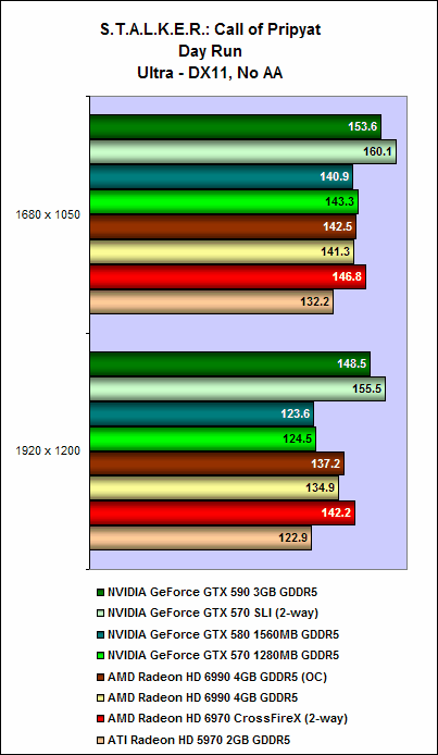
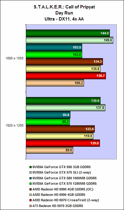
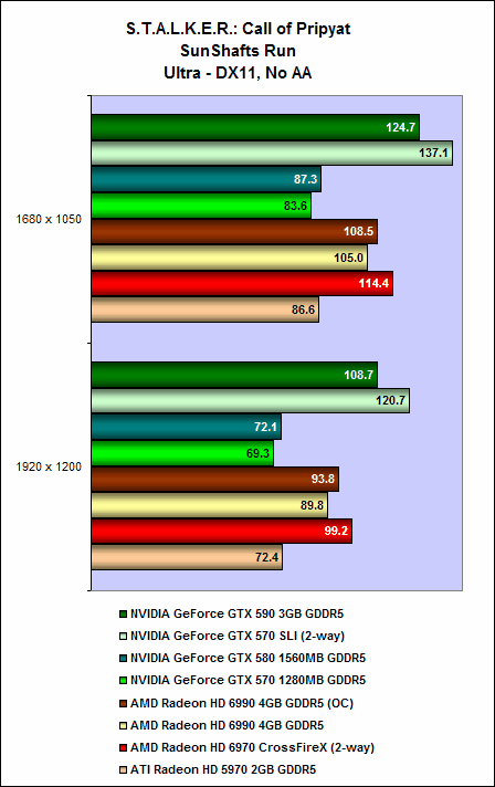
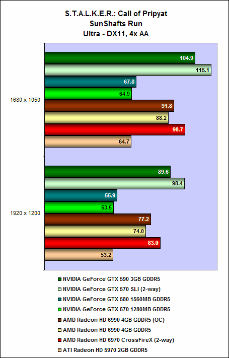
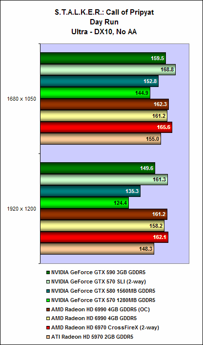
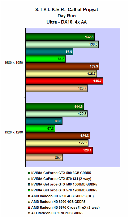
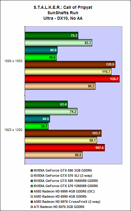
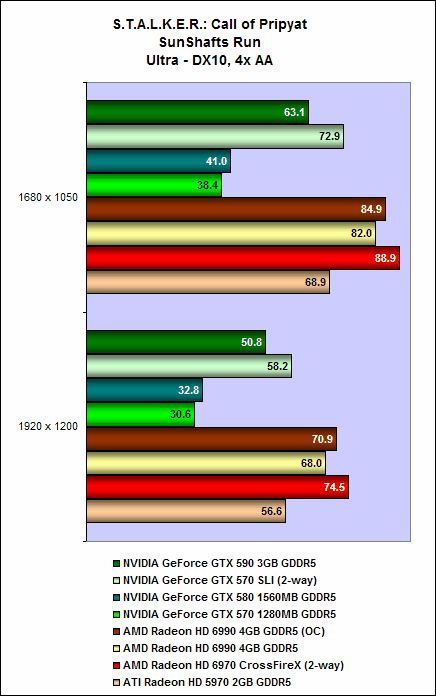
S.T.A.L.K.E.R.: Call of Pripyat Results
On S.T.A.L.K.E.R.: Call of Pripyat, the GeForce GTX 590 managed a comeback and racked up higher frame rates when running in DirectX 11 and with tessellation enabled. On the Day runs, it was about 10% faster than the competing Radeon HD 6990 and it extended its lead coming to the Sun shaft runs by almost 20%.
The tables turned when we reverted to DirectX10 and disabled tessellation. Here on the Day runs, the Radeon HD 6990 was quicker than the GeForce GTX 590, but on the Sun shaft runs, it was more than a whopping 30% faster. This shows that the Radeons are better optimized for DirectX10 applications - which far outnumber DX11 games availability.
DirectX 11 Results
 |  |
 |  |
DirectX 10 Results
 |  |
 |  |
Temperature
Heat has always been the bane of dual-GPU cards but the NVIDIA GeForce GTX 590 fared pretty well in this aspect as we recorded a maximum operating temperature of 70 degrees Celsius, which is pretty impressive for a dual-GPU card of its caliber. Much of this has got to do with the extensive cooling features which NVIDIA implemented on the card such as the 12-layer copper-infused board, cooling plates, and dual copper vapor chambers.

Power Consumption
Power consumption figures of the GeForce GTX 590 were pretty in line with our expectations. A maximum sustained reading of 451W was recorded and although that’s significantly less than two GeForce GTX 570 in SLI, it’s marginally more than the Radeon HD 6990.

Overclocking
Using MSI’s competent Afterburner overclocking utility, we managed to push the GeForce GTX 590 up to a maximum overclocking state of 680MHz at the core and 3800MHz DDR - an increase of 73MHz and 386MHz DDR respectively. This gave us 20891 3DMarks on the Extreme preset, a decent improvement of 8%.

What Could Have Been...
NVIDIA has enjoyed a pretty good run of late ever since refreshing its Fermi lineup with the GeForce GTX 500 series. The GeForce GTX 580 finally brought about the full 512 CUDA cores that Fermi promised, and the GTX 570 with its tweaked GF110 chip is a very much improved version of the old GeForce GTX 480. NVIDIA followed up this year with the GeForce GTX 560 Ti, which forced its rivals to make considerable revisions in its pricing strategy, and next, refreshed the mainstream segment with the GeForce GTX 550 Ti.
Unfortunately, the new GeForce GTX 590 bucks this trend and is yet another ho-hum release from NVIDIA. Let’s address its performance first. Considering it has two 512-core GF110 chips as its main ingredients, its performance is underwhelming, to say the least. In most cases, it trailed AMD’s dual-GPU Radeon HD 6990, its main competitor in this segment of the market. And given that AMD was first to launch its dual-GPU flagship card, we fully expected NVIDIA to one-up them where raw performance is concerned, but that is unfortunately not the case. In the end, the fact that GeForce GTX 590 is only about as quick as two GeForce GTX 570 cards in SLI, goes to show how much NVIDIA has downclocked the two GF110 cores in the GeForce GTX 590.
However, while its performance didn’t exactly set the stage on the fire, it does excel in other aspects. For one, it is remarkably quiet as dual-GPU card, much more so compared to the Radeon HD 6990. It’s not dead silent though, but at least you won’t require headphones like you would with a Radeon HD 6990 at full speed. On top of that, it also runs pretty cool (for a dual-GPU card at least). This is a testament to the efficiency and effectiveness of NVIDIA’s new cooler design.
Despite the rather effective cooler, NVIDIA says that should you decide to SLI this beast, it’s highly advisable to leave an expansion slot free, lest the card behind be starved of air. While enthusiasts usually leave a gap when using dual graphics cards, this is probably the first time we're seeing it as a mandatory requirement. Like the Radeon HD 6990 then, this makes the GeForce GTX 590 somewhat difficult or at least troublesome to SLI, even if NVIDIA has provided a list of GeForce GTX 590 Quad SLI certified motherboards.
Additionally, it is also the first Fermi card to support more than two displays simultaneously, and crucially, also the first card to be able to handle 3D Vision Surround on its own. With this in mind, it’s probably the easiest and most fuss-free solution for anyone looking to get started on building a 3D Vision Surround rig.
At US$699, the GeForce GTX 590 is priced almost exactly to match AMD’s Radeon HD 6990. In terms of performance, it might be the slower of the two, but the difference is probably not sufficient to lose sleep over. Not surprisingly, it also costs about the same as two GeForce GTX 570 cards.

The GeForce GTX 590 is the best single graphics card NVIDIA has to offer, but we can't help but feel that its potential hasn't been fully fulfilled.
To summarize, we are disappointed with the GeForce GTX 590, mainly because of its performance. With dual 512-core GF110 GPUs, we expected performance that would mirror or at least shadow that of two GeForce GTX 580 in SLI. However, the GeForce GTX 590 is more comparable to two GeForce GTX 570 in SLI. Of course, a single GeForce GTX 580 is more expensive at around US$500 a pop, but had NVIDIA achieved GeForce GTX 580 SLI levels of performance, we’re sure extreme users wouldn't mind coughing up a full grand for the card.
What’s more frustrating though, is that the only thing keeping NVIDIA from fulfilling and reaching that levels of performance is simply the clock speeds. At the end of the day, the GeForce GTX 590, like the Radeon HD 6990, is a card that asks “what if”. What if, we could run it at the full clock speeds that a single GPU was designed to run at? What kind of performance would we get?
So, despite the hardcore intentions of the GeForce GTX 590, it ends up, like its rival from AMD, a card fraught with compromises. Heat, noise and power, remain the bane of high-end cards, and in that respect, the GeForce GTX 590 represents what NVIDIA can achieve on a single PCB. Perhaps someone can jury-rig a liquid-cooled overclocked solution that can fulfill its potential.
Sadly, it's not the fastest single graphics card in the market, so those gunning for outright single card performance might want to consider AMD’s Radeon HD 6990, as it is slightly quicker, but if 3D Vision Surround intrigues you and you don’t mind the slight disadvantage in raw frame rates, the GeForce GTX 590 is an option. Those looking for raw performance no matter the cost will have to settle for multiple graphics cards as it now appears that both AMD and NVIDIA cannot deliver what they require.
Our articles may contain affiliate links. If you buy through these links, we may earn a small commission.