
Fermi Arrives - NVIDIA GeForce GTX 480
After a long, long wait, Fermi is finally here in the form of the GeForce GTX 480. We put the card through its paces to see how it matches against ATI's finest, how much faster is it compared to its predecessor.

Fermi Here, At Last
In September last year, ATI kick-started the next round of graphics war with the release of their Evergreen series of graphics cards. Spearheaded by the awesome Radeon HD 5870, which is powered by the massively powerful Cypress XT GPU, ATI's Evergreen heralded a new generation of graphics performance and efficiency.
Not only that, with Evergreen, ATI also introduced something called EyeFinity, which allowed for multi-monitor setups. Right out of the box, all Evergreen cards from the flagship Radeon HD 5970 right down to the Radeon HD 5450 are all capable of driving up to three displays simultaneously. There were also the special EyeFinity6 versions, which allowed a single card to drive six monitors in tandem. EyeFinity, though possibly niche, was much welcomed, especially by gamers who wanted a more immersive experience; as well as corporate users, who wanted an affordable means of expanding their desktop real estate.
With so much coming from the red camp, we were naturally intrigued to see what NVIDIA had to offer. Shortly after ATI announced Evergreen, NVIDIA countered with their own GPU Technology Conference in San Jose, California. At the conference, NVIDIA CEO Jen-Hsun Huang, unveiled the new architecture, codenamed Fermi, that would be the driving force behind NVIDIA's latest graphics cards.

NVIDIA CEO Jen-Hsun Huang shows off the company's latest and most advanced GPU yet.
Needless to say, the event generated a lot a bit of buzz. And who could forgot the incident where eagle-eyed tech journalists the world over noticed something amiss in the PR photos NVIDIA sent out. In the end, NVIDIA had to admit that the card that was shown on stage wasn't real. However, they did insist that all demos ran at the event were in fact powered by Fermi cards. That created quite a stir, of course, but one that is not entirely unexpected since it just goes to show how far we are from seeing the cards on store shelves. To be fair, NVIDIA never promised anything anytime soon and it was just a showcase of the new GPU technology that was shared at the event. That said, the tech media elsewhere and the enthusiasts were really debating over nothing in our opinion.
Two months later in December, we posted news with regards to 40nm yield issues at TSMC affecting supplies of both ATI and NVIDIA graphics card. Back then, word on the street was that Fermi would have to wait until March to see the light of day. With the benefit of hindsight, they were right on the money.
It's March now, and Fermi is finally here - nearly six months after NVIDIA CEO Jen-Hsun Huang first showed the world the new Fermi architecture; and after ATI has released their entire line-up of Evergreen cards. To say that NVIDIA was slow to the competition would perhaps be a bit of an understatement. But as the old saying goes, “better late than never”, so what exactly can we expect?
Head over to the next page to find out.
Fermi Architectural Highlights
First and foremost, with Fermi, NVIDIA is taking a significantly different direction as to where GPU technology is headed. Sure, NVIDIA assures that the new chips will still be efficient where gaming is concerned, but with Fermi, NVIDIA is taking aim also at high performance computing (HPC). Which is no surprise given that they have spent so much time, effort and money into promoting its CUDA architecture as a means of speeding up applications that are suited to be executed in parallel by multiple cores. For more about CUDA, we refer you to an earlier article we've written .

With Fermi, NVIDIA is hoping to snag a larger piece of the GPU computing pie.
Fermi represents NVIDIA's first high-end chip to be manufactured using a 40nm processor and with over 3 billion transistors onboard, it is also NVIDIA's biggest and most ambitious yet. However, it is evolutionary rather than revolutionary, seeing that it still has its roots in the original G80 chip that debuted back in 2006, and we've highlight its most significant enhancements here:
GigaThread Engine
In essence, Fermi works in very much the same way as NVIDIA's previous generation GT200 and G80 chips. Commands from the CPU are read by the GPU via the host interface, after which the GigaThread Engine copies the data from the system memory and onto the frame buffer, and then creates and dispatches thread blocks to the various Streaming Multiprocessors (SMs). The SMs in turn schedule "warps" (groups of 32 threads) to the CUDA cores (shader processors) and other execution units. Hence, rather than radically changing the way Fermi works, NVIDIA has sought to streamline and make processes more efficient and quicker instead. The basic underlying reason of why the GigaThread Engine exists and how it works is still similar to that of the G80 chips in 2006 - only much more capable now.

Concurrent kernel execution helps speed things up by ensuring no cores are left idle.
As we've mentioned earlier, the efficiency of the GigaThread Engine is crucial to performance and the Fermi architecture improves on the GigaThread engine by providing greater thread throughput by means of enabling faster context switching, more refined thread scheduling, and most importantly, concurrent thread execution. The end result is greater speed and efficiency in the scheduling and dispatching of threads to the shader multiprocessors (SMs), which will benefit not only GPU computing processes, but also 3D gaming too.
Streaming Multiprocessors (SM)

An overview of the shader multiprocessor found in Fermi.
Speaking of SMs, Fermi is made up of 16 of them, each with 32 shader cores configuration for a grand total of 512 CUDA cores - which is more than twice the number the GeForce GTX 285 packs (240, in case you were wondering). And just for comparisons sake, it's four times the number of shader cores on the original grand-daddy of the current architecture, the GeForce 8800 GTX.
One of most important changes to these CUDA cores is that they have been specifically engineered to perform better on double precision applications. Such a change was brought about because of requests by NVIDIA's partners in GPU computing, where double precision performance is critical. Fermi also implements the new IEEE 754-2008 floating-point standard, and has been specifically engineered to offer greater performance in double precision operations. NVIDIA claims that performance on double precision applications can be as much as 4 to 8 times faster on Fermi compared to the older GT200.
Memory Subsystem
To make the SMs even more efficient, NVIDIA has also made changes to the memory subsystem, one of which is to provide a larger and more flexible L1 cache. While the older GT200 chip only had 24KB of L1 cache, Fermi makes do with 64KB, and this can be configured as either 16KB of shared memory and 48KB of cache or as 48KB of shared memory and 16KB of cache. In addition, all 16 SMs will have access to an unified 768KB of L2 cache, which is markedly larger than the GT200's 256KB L2 cache. All in all, these changes help make Fermi a better performer at HPC applications.
That aside, the new Fermi GPU will also have six channels of 64-bit wide GGDR5 memory controllers, which means a net memory bus width of 384 bits. This is down from the 512 bits wide memory bus interface on the older GT200. However, the support for GDDR5 memory (a first for NVIDIA's high-end GPU), which delivers twice the bandwidth compared to GDDR3, should make up the difference. Theoretical memory bandwidth of the GeForce GTX 480 is 177.4 GB/s as compared to the GeForce GTX 285's 159 GB/s.
On top of this, the new GPU will be the first in the world to support ECC (Error-correcting code) and will also be capable of supporting up to 6GB of memory. ECC and 6GB of memory are probably redundant for gaming, but will offer great appeal to corporations and educational institutions who rely on GPUs for high performance precision computing needs.
As we have seen, most of the new implementations on Fermi are geared towards HPC users, so what does it actually mean for gamers? Fret not, because gaming is still very much in NVIDIA's blood and for that, we have to turn to the next page for NVIDIA's first chip featuring Fermi – the GF100.
Meet the GF100
All in all, the new architecture is one that has clearly been setup to perform well for HPC needs, but how will it perform on your normal games? Well, that's what we are here to find out.

The GF100 is the physical manifestation of the Fermi architecture. NVIDIA says this will reclaim the crown of world's fastest GPU.
NVIDIA's latest top dog is the GeForce GTX 480 and in it will be the all-new GF100 GPU, the first GPU to make use of the new Fermi architecture. The GF100 chip will boast 480 CUDA cores, 60 texture mapping units and 48 raster operating units. In terms of clock speeds, the core will operate at 700MHz, whereas the shaders and memory are at 1401MHz and 3696MHz DDR respectively.
Observant readers will no doubt notice that 480 CUDA cores is 32 short of what NVIDIA claims will be found in Fermi. Does this mean a possible 512-core variant of the GeForce GTX 480 in future? When quizzed, NVIDIA did not say why the GF100 features 480 cores instead of the 512 as stated earlier, but many are speculating that this could be because of poor yields due to the complexity of the new chip. To add, NVIDIA also did not explicitly deny the possibility of a 512-core variant in future - now this is interesting. Factor in NVIDIA's penchant for releasing an updated top model of the same GPU architecture and it becomes apparent that an even more capable version is likely in the making.
Anyhow, launching along side the GeForce GTX 480 is the GeForce GTX 470. The GeForce GTX 470 has a scaled down version of the GF100 chip, with an entire SM disabled. This means 448 CUDA cores, 56 texture mapping units and 40 raster operating units. It gets lower clock speeds as well. Its core is running at 607MHz, while shaders and memory at 1215MHz and 3348MHz DDR respectively. We'll share with you our findings of the GTX 470 in the coming weeks, but for now here's how the GF100, specifically the GeForce GTX 480 stacks up against the competition.
Model | NVIDIA GeForce GTX 480 1536MBGDDR5 | ATI Radeon HD 5870 1GB GDDR5 | ATI Radeon HD 5970 2GB | NVIDIAGeForce GTX 285 1GBGDDR3 | NVIDIA GeForce GTX 295 1729MBGDDR3 |
Core Code | GF100 | Cypress XT | Hemlock XT | GT200 | GT200 |
Transistor Count | 3200 million | 2150 million | 4300 million | 1400 million | 2800 million |
Manufacturing Process | 40nm | 40nm | 40nm | 55nm | 55nm |
Core Clock | 700MHz | 850MHz | 750MHz | 648MHz | 576MHz |
Stream Processors | 480 Stream Processors | 1600 Stream processing units | 3200 Stream processing units | 240 Stream Processors | 480 Stream Processors |
Stream Processor Clock | 1401MHz | 850MHz | 725MHz | 1476MHz | 1242MHz |
Texture Mapping Units (TMU) or Texture Filtering (TF) units | 60 | 80 | 160 | 80 | 160 |
Raster Operator units (ROP) | 48 | 32 | 64 | 32 | 56 |
Memory Clock | 3696MHz GDDR3 | 4800MHz GDDR5 | 4000MHz GDDR5 | 2484MHz GDDR3 | 1998MHz GDDR3 |
DDR Memory Bus | 384-bit | 256-bit | 256-bit | 512-bit | 448-bit |
Memory Bandwidth | 177.4GB/s | 153.6GB/s | 256GB/s | 159.0GB/s | 223.8GB/s |
PCI Express Interface | PCIe ver 2.0 x16 | PCIe ver 2.0 x16 | PCIe ver 2.0 x16 | PCIe ver 2.0 x16 | PCIe ver 2.0 x16 |
Molex Power Connectors | 1 x 6-pin, 1 x 8-pin | 2 x 6-pin | 1 x 6-pin, 1 x 8-pin | 2 x 6-pin | 1 x 6-pin, 1 x 8-pin |
Multi GPU Technology | SLI | CrossFireX | CrossFireX | SLI | SLI |
DVI Output Support | 2 x Dual-Link | 2 x Dual-Link | 2 x Dual-Link | 2 x Dual-Link | 2 x Dual-Link |
HDCP Output Support | Yes | Yes | Yes | Yes | Yes |
Street Price | Launch Price: US$499 | ~US$399 | ~US$599 | ~US$350 | ~US$500 |
Other Features of the GF100 GPU
Apart from adding extra CUDA cores, NVIDIA has also made improvements to other aspects of the chip and added 3D Vision Surround functionality. Here are the highlights:
GPC Architecture
One of the main features that the DirectX 11 API brings about is tessellation, which increases the number of polygons visible in real time dynamically by means of complex algorithms. This results in greater detail and translates to a higher level of realism.
However, the use of tessellation changes the GPU's workload balance and to counter it, NVIDIA has to reorganize the GF100's internal architecture a little and also introduced a new geometry engine.

Each GPC is a mini-GPU of sorts, and the GeForce GTX 480 has four of them.
Firstly, graphics Processing Clusters (GPCs) are the GF100's dominant high-level hardware block. Each GPC is made up of four SMs sharing a single raster engine, and handles all vertex, geometry, raster, texture and pixel processing operations.
A new geometry engine called the Polymorph Engine was also introduced. Each SM has its own Polymorph engine, which in turn has its own dedicated vertex fetch unit and tessellator. Hence, the GF100 has 15 Polymorph engines alogether, which NVIDIA claims will enable breakthrough tessellation performance.
Texture Units
One way the GF100 is faster is that each SM has now got four dedicated texture units and a dedicated texture cache. Previously in the GT200, three SMs shared a single texture engine, which in turn has eight texture filtering units. This makes the GF100 is more efficient, and on top of that, NVIDIA also says that the internal architecture of the texture units has been enhanced.
And as we've have mentioned earlier, the dedicated L1 texture cache is now more flexible and the large 768KB L2 cache means that the maximum cache size for textures is now three times greater than the GT200. This will benefit games which are running texture-heavy shaders.
Raster Operating Units
We know that enabling anti-aliasing improves graphics quality, but that comes at the price of lower performance. With the new GF100, NVIDIA aims to improve anti-aliasing performance by reducing the performance hit that affect systems when gamers turn on anti-aliasing in their games.
To achieve that, NVIDIA has redesigned the GF100's ROP (raster operating partitions) subsystem for greater throughput. The GF100's ROP partition contains eight individual ROP units, which is twice as much as previous architectures. These units can output a 32-bit integer pixel per clock; an FP16 pixel over two clocks or an FP32 pixel over four clocks. NVIDIA states that the GF100 chip is geared specifically to tackle 8x MSAA, which means enabling anti-aliasing on your games will result in a lesser hit in performance.
NVIDIA 3D Vision Surround

Costly yes, but for 3D gaming, this is as good as it gets.
Enhanced texture and raster operating units aside, perhaps the most exciting feature that the GF100 brings is NVIDIA 3D Vision Surround. To be sure, this feature is not exclusive to the GF100 since NVIDIA says support will be extended also to the GT200 series of cards, but nevertheless, what it does is offer stereoscopic 3D gaming on three monitors.
The end result should be fantastic, going by how well the original GeForce 3D Vision kit performed. The only inhibiting factor we can think of is price. Considering that the new NVIDIA cards are incapable of driving three monitors simultaneously, 3D Vision Surround demands a SLI setup. Considering that the 3D workload has also increased tri-fold, that also necessitates the reason why an SLI setup is needed for 3D Vision Surround. Also, you'll need monitors with a refresh rate of at least 120Hz. All in all, the costs involved in getting a 3D Vision Surround system setup is going to be considerable.
Evidently, NVIDIA has done much to Fermi and the GF100 to beef it up for the next-generation of games. But talk is cheap as they say, so how does it actually perform in real-world applications? We'll find out soon enough.
The NVIDIA GeForce GTX 480
The GeForce GTX 480 is NVIDIA's latest flagship and the first to make use of the new GF100 chip.The first thing you'll probably notice about the GeForce GTX 480 is how big the card is. As you'll see from the photos below, it is roughly the length of a Radeon HD 5870, but it has a meaner looking reference cooler, which makes it look more imposing and perhaps slightly larger. What also grabs your attention are the four thick heat pipes sprouting from the core. Such a design is a break from reference coolers of old, which have traditionally been blockish and dull.
Anyhow, feast your eyes on the photos of the GeForce GTX 480.

Small the GeForce GTX 480 ain't, and it looks very different from reference NVIDIA cards of old thanks to the new cooler design.

Length-wise, the GeForce GTX 480 and the Radeon HD 5870 is about the same, but the Geforce GTX 480 looks a tad stockier.

This is what the back of the cards look like. It has the same cut outs as we've seen on the dual-GPU GeForce GTX 295.

Our reference card sports the usual double DVI ports and also quite oddly, a mini-HDMI port.

The four thick heat pipes are a necessity seeing that the card has a rated TDP of 250W. In comparison, a Radeon HD 5870's rated TDP is only 188W. One can also see the two SLI connectors - the GeForce GTX 480 is 3-way SLI compatible.

The GeForce GTX 480 is powered via a 6 and 8-pin PCIe power connector. NVIDIA also recommends that users pair it with a PSU rated for at least 600W.
Test Setup
To see how the new GeForce GTX 480 matches up, we'll be using an Intel X58 and Core i7 setup with the following specifications:
Intel X58 Test System:
- Intel Core i7-975 (3.33GHz)
- Gigabyte GA-EX58-UD4P motherboard
- 3 x 1GB DDR3-1333 OCZ memory in triple channel mode
- Seagate 7200.10 200GB SATA hard drive
- Windows 7 Ultimate
Obviously, the GeForce GTX 480's main rival is ATI's Radeon HD 5870, and we'll be paying close attention to how the two cards perform. Another key point of interest is how much faster the GeForce GTX 480 will be compared to the older GeForce GTX 285. With all the improvements that NVIDIA claims, it'll be intriguing to see what it translates to in actual frames per second. That aside, we've also included other high-end cards such as the Radeon HD 5970, HD 5850 and the GeForce GTX 295, to see just where the GeForce GTX 480 stands amongst its high-performance peers.
The full list of cards tested and drivers used are as follows:
- NVIDIA GeForce GTX 480 (ForceWare 197.17 Beta)
- NVIDIA GeForce GTX 295 (ForceWare 196.21)
- NVIDIA GeForce GTX 285 (ForceWare 196.21)
- ATI Radeon HD 5970 (Catalyst 10.2)
- ATI Radeon HD 5870 (Catalyst 10.2)
- ATI Radeon HD 5850 (Catalyst 10.2)
- ATI Radeon HD 4890 (Catalyst 10.2)
We've also tweaked our suite of benchmarks a little. Three new inclusions are the immensely popular Battlefield Bad Company 2, the Heaven benchmark from Unigine, and S.T.A.L.K.E.R.: Call of Pripyat. These three new benchmarks were included because they take full advantage of DirectX 11, allowing us to see how the cards cope with the newer DirectX 11 games. We will also test them on DirectX 10 settings to fully discern how the new generation cards compare to the old on the newer DirectX 11 games and also just how much tessellation affects performance.
We have also adjusted our testing resolutions to reflect 16:10 aspect ratio widescreen monitors that are widely (no pun intended) in use today.
The full list of benchmarks used:
- Futuremark 3DMark Vantage
- Crysis Warhead
- Far Cry 2
- Warhammer: Dawn of War 2
- Battlefield Bad Company 2
- "Heaven" from Unigine
- S.T.A.L.K.E.R.: Call of Pripyat
3DMark Vantage Results
We begin our analysis as we usually do with 3D Vantage, and the GeForce GTX 480 is off to a lacklustre start. Although it was quicker than the Radeon HD 5870 on the High and Extreme presets, the difference was only about 3%. The Radeon HD 5970 remains to be the top dog, while the older GeForce GTX 295 still remains highly competitive.

Crysis Warhead & Far Cry 2 Results
The GeForce GTX 480 began to flex its muscles on Crysis Warhead, outperforming the Radeon HD 5870 by an average of around 10%. It also gets the distinction of being the only single GPU card capable of breaching the magical 30fps mark on the most intense setting of 1920 x 1200 with 4x anti-aliasing enabled. Although the Radeon HD 5870 is just slightly behind, it's still quite an achievement, nonetheless. Again, the Radeon HD 5970 is the one to beat, and we also noted that the performance of the GeForce GTX 480 is comparable to that of the GeForce GTX 295.


On Far Cry 2, the Radeon HD 5870 was absolutely massacred by the GeForce GTX 480, as it was an astonishing 40 - 50% quicker. In fact, with anti-aliasing enabled, it was able to outperform even the Radeon HD 5970, which up till now, had been the quickest card. It was also markedly faster than the older GeForce GTX 295 and nearly twice as quick as the GeForce GTX 285.


Dawn of War 2 & Battlefield Bad Company 2 Results
The GeForce GTX 480 didn't do too well on Dawn of War 2, finding itself pipped by the Radeon HD 5870, albeit by a very slight margin. The Radeon HD 5970 was the top performer, but its oddly consistent scores seem to suggest that it was bottlenecked by the CPU.

Interestingly, NVIDIA claims that when running Dawn of War 2, ATI cards by default demote the FP16 render targets to R11G11B10 render targets, which are half the size and less accurate. Admittedly, NVIDIA says that the change in quality is subtle, but it does have an affect on performance. We decided to investigate this claim by disabling Catalyst AI and found that it does affect performance by a considerable margin. Suffice to say that most users will normally be running with Catalyst AI enabled so this comparison below while technically correct, it's not representative of actual usage. Furthermore, since quality differences are small, it again makes sense for ATI to offer more performance.

Battlefield Bad Company 2 is one of the new benchmarks we are introducing and it is widely praised for its stunning graphics. It is a DirectX 11 game, but unfortunately the graphics settings are really basic, with no controls to allow for choosing which API to use or even enabling or disabling tessellation.
Here, the GeForce GTX 480 blitzed the Radeon HD 5870 by a significant margin. It was more than 20% quicker than the Radeon HD 5870 on both runs, and wasn't that far off the mark from the Radeon HD 5970. Note that the older generation cards maintained playable frame rates despite the intensive settings used.

Unigine "Heaven" Results
Unigine's “Heaven” benchmarks was one of the first DirectX 11 benchmarks to surface. Although the practicality of this benchmark has been debated in a previous article, it is still a good gauge of a card's ability to handle tessellation-heavy operations. Running using the DirectX 11 API and enabling tessellation saw the GeForce GTX 480 monstered its way past the Radeon HD 5870, putting it within striking distance of the Radeon HD 5970.
Running again, this time with DirectX 10 and therefore no tessellation, we can see that the performance between the GeForce GTX 480 and Radeon HD 5870 is highly comparable. However, what's important to note is that if you compared the DirectX 11 and DirectX 10 sets of results, you'll notice that the Radeon HD 5870 suffers a bigger drop in performance when tessellation is enabled. Clearly, the enhanced architecture of the GF100 chip is paying dividends where tessellation is concerned.


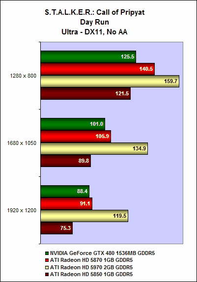
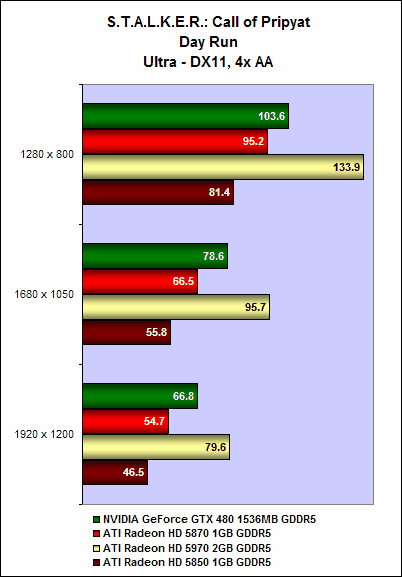
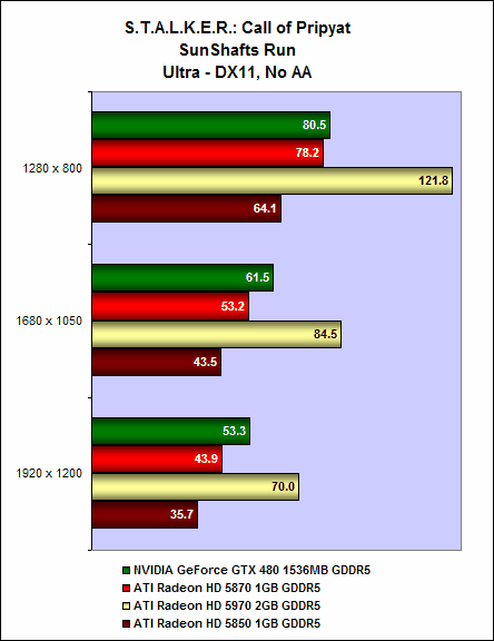
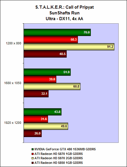
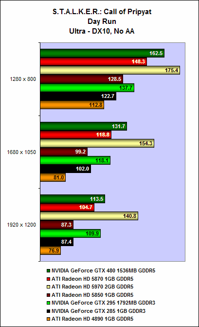
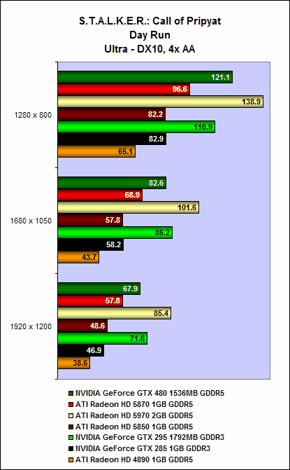
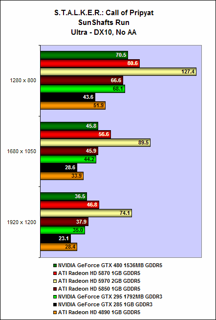
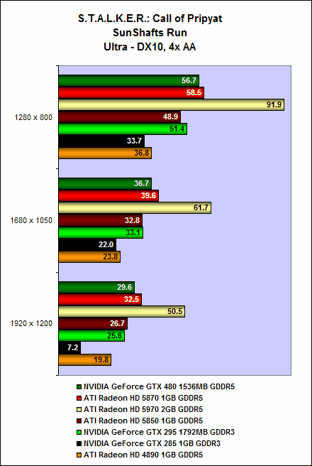
S.T.A.L.K.E.R.: Call of Pripyat Results
S.T.A.L.K.E.R.: Call of Pripyat is yet another DirectX 11 game, which features real-time tessellation, which we're testing with for the first time. Again, we'll run it once with DirectX 11 and tessellation enabled, and another time with DirectX 10 and no tessellation. We'll be looking at results from the Day run, which is a fly-through of the game's environment, as well as from the Sun Shafts run, which is the same fly-through except this time with a brightly lit sun, showcasing the game's HDR lighting and dynamic soft shadows rendering.
Both cards are highly competitive on this game, but it was the GeForce GTX 480 that came on top most of the time. However, it is interesting to note that this time, however, it was the Radeon HD 5870 that suffered the least performance drop. We noted that it managed nearly similar frame rates on both the Day and Sun Shafts with or without DirectX 11 and enabling tessellation.
The GeForce GTX 480, though faster, was somewhat erratic. On the Sun Shaft runs, we noticed that it was actually slower when DirectX 11 and tessellation was disabled. This could be due to the beta nature of the drivers in use and will be something that we'll be keeping a look out for in future tests.
DirectX 11 Results
DirectX 10 Results
Temperature
With a maximum recorded operating temperature of a whopping 92 degrees Celsius, the GeForce GTX 480 is the hottest reference card we've seen in recent years. And it is apparent that the chunky reference cooler is a necessity. At 92 degrees Celsius, it is also operating dangerously close to its threshold of 105 degrees Celsius.
Here's a point to note though, since the drivers we used for the GeForce GTX 480 were still in beta, this could be a problem of poor power optimization that could possibly be corrected in future driver releases. However, if our experience is anything to go by, improvements in driver revisions have little to no effect when it comes to aspects like heat and power consumption.
Power Consumption
While the GeForce GTX 480 offers unparalleled single-GPU performance, it also has an unmatched hunger for power. It's peak reading of 332W eclipses that of the Radeon HD 5870 and even the Radeon HD 5970, which has two GPUs! It seems then that NVIDIA has done little to improve on the power efficiency of their new cards. Again, take note that this could be due to poor driver optimization, but as we've mentioned above, we wouldn't bet on it.
NVIDIA's defence on the subject of power consumption is their performance-per-watt efficiency where in DX11 games, their card's much higher performance would give much better figures in the ratio aspect. A lot of the Fermi architecture was geared for the future with DX11 heavy titles and as such running DX10 and DX9 game titles would result in a lacklustre outcome for power consumption. While this rationale is somewhat true going by the performance numbers we've attained, what we can say is that it doesn't alter the absolute measured power consumption figures. Still, we would take this chance to test more games and applications in our spare time, but going by our usual base of comparison that's normally a good representation, the GeForce GTX 480 seems to consume too much power. It's saving grace however is that at times its performance numbers are as high as the dual-GPU Radeon HD 5970, so it's probably not too bad.

Really Fast, But Not Much Else
Technically, the GeForce GTX 480 is an evolutionary step above the GT200. It adds more hardware and gets a few internal tweaks here and there to make it for suitable for HPC computing purposes and to better handle the latest DirectX 11 games.
Looking at the GeForce GTX 480's performance, the results are certainly positive, as there's no doubting the GeForce GTX 480's ability to crunch graphics. It has reclaimed the title of the world's fastest single GPU card from ATI and by some margin too, seeing that it can be as much as 50% quicker than the Radeon HD 5870 in some tests. In fact, it's so quick that it is enough to even give the Radeon HD 5970 something to think about. The GF100 is nothing less than a monster GPU, but given that it is nearly half a year late to the competition, would you expect anything less?
Blazing performance aside, we are somewhat worried about the exceedingly high TDP ratings for the new GeForce GTX 480. With its rated TDP of 250W, it is considerably more power hungry than compared to the Radeon HD 5870. And although ATI has given its dual-GPU Radeon HD 5970 a higher rated TDP of 294W, we found in our tests between the two that it was the GeForce GTX 480 who consistently recorded higher power draw figures. Heat is another issue, seeing that the card recorded a maximum operating temperature of 92 degrees Celsius, which is possibly the highest we've seen yet from any graphics card. Sure, these problems may be rectified by driver revisions, but the chances of it happening is small going by our past experience in this field. As it is, it seems that power efficiency was not one of NVIDIA's design priorities, and we wonder how that will affect the mainstream and budget cards based off the GF100 chip, when it does come.
Speaking of which, apart from the GeForce GTX 470 which was launched along side the GeForce GTX 480, NVIDIA did not explicitly state their plans for future cards that will make up the GTX 400 series. Of course, that is not to say that there won't be any mainstream GTX 400 cards, but we can't help but be reminded of what happened with the GTX 200 series, where NVIDIA was content to just rename older products and pass them off as new mainstream editions. The GTS 250, which was really a GeForce 9800 GTX+, was one such example of NVIDIA's penchant for renaming old products.

Supremely fast, with a price to match. However, its high power requirements and absurd operating temperatures mean it's not for everyone. Strictly hardcores only.
To end, there's no questioning the sheer graphics horsepower of the card, but performance aside, we don't believe it offers much more than existing Radeon 5800 series cards. The Radeon 5870 may no longer be the fastest single GPU card, but it is more than capable of handling today's games at maximum settings. And 3D Vision Surround, as good as it sounds, is really nothing more than a driver upgrade, seeing that the same can be attained with older GTX 200 cards.
Therein lies the problem with the GeForce GTX 480. If you had gone out and gotten yourself a Radeon HD 5870 or HD 5850 in the months before, you won't feel any sense of regret, much less the urge or need to upgrade to a GeForce GTX 480. This is even more so when you consider the price. At a launch price of US$499 (S$700), the GeForce GTX 480 costs a whopping US$120 more the Radeon HD 5870.
All things considered, the GeForce GTX 480 is best described as a supremely high-end premium graphics card for those who care for nothing other than getting the highest possible performance off a single GPU.
Those looking for something more accessible and reasonably balanced should stick to the Radeon HD 5000 series or they can turn to the new GeForce GTX 470, a toned down version of the GeForce GTX 480. It packs lesser hardware and slower clock speeds and is priced at a more enticing US$349 (S$490). Stay tuned for our evaluation of it.
Our articles may contain affiliate links. If you buy through these links, we may earn a small commission.