
GeForce GTX 680 - NVIDIA's 28nm Successor to Fermi
Since Kepler was made known in October 2010, we have waited with bated breath for its arrival. Its manifestation in the form of a NVIDIA GeForce GTX 680 graphics card reached our offices and has managed very interesting performance results with its new architecture. Read on!

GeForce GTX 680 - Stating Kepler's Laws
Since its announcement in October 2010 at NVIDIA's GPU Technology Conference (GTC), Kepler, the successor to Fermi, has kept us waiting in bated breath for its arrival. Today, 22nd March 2012, marks its official launch and marks the first salvo of retaliation by NVIDIA to AMD's Southern Island series of GPUs. Like AMD's latest GPUs, Kepler is based on the 28nm fabrication process and is currently touted to be the fastest and most power efficient GPU. AMD had the first-to-market advantage and the card manufacturers wasted no time in getting their wares based on the Radeon HD 7900 GPU series and Radeon HD 7700 GPU series to their different target markets. We feel that NVIDIA has some catching up to do in this race as it reveals its first manifestation of Kepler in the form of the GeForce GTX 680.

The die shot of GeForce GTX 680 GPU with an area of 294 square mm. Its die size has shrunk about 43% when compared to GeForce GTX 580; however, GTX 680 packs in 3.54 billion transistors versus GTX 580 transistor count of 3 billion!
The GeForce GTX 680 is positioned to be the most power efficient flagship GPU, claiming this title from its older GeForce GTX 580 when it too touted similar claims in its heyday. According to technical information gleaned during our visit to NVIDIA GeForce Editor's Day 2012, the architecture of Kepler is actually positioned as an improvement from the GF114 core of GeForce GTX 560 as the GTX 560 is the latest from NVIDIA's GeForce 500 series GPUs. Using that GPU architecture as the base, NVIDIA designed the GK104 core that makes up the GeForce GTX 680.
Now for the techies, some of you might have long guessed from the core code that this the GTX 680 isn't the true flagship and there is some truth to this looking at the rumors on the grapevine and from our close discussions from NVIDIA. However with no official word and the fact that the GeForce GTX 680 can is positioned to compete with the top Radeon HD 7900 series single GPU graphics card, for all intents and purposes, the GeForce GTX 680 is their current flagship. There are three guiding principles in the development of the Kepler architecture and they are summed up neatly in a triplet of adjectives: Faster, Smoother and Richer.
Kepler's First Law - Faster
One of the most important hardware feature of the Kepler GPU is its four new Graphics Processing Clusters (GPC). This term was first used in Fermi's architecture which also featured four GPC units. A GPC is basically an independent block of processing engines that can exist on its own as it contains all the necessary processing stages within its cluster. While the number of GPC units haven't changed in all these years, the hardware and configuration within each GPC has changed drastically. Within each GPC of the GeForce GTX 680 resides the next generation Streaming Multiprocessor (SMX).

Each pair of GPCs is separately by the L2 cache that has a capacity of 512KB. Take note of the next generation SMX packs in 192 CUDA cores, an increment of 160 CUDA cores over the previous SM. Incidentally, the CUDA cores in both generations of the the Streaming Multiprocessors share the same kind of CUDA core as they've not evolved. Instead, the performance per watt ratio has been drastically improved on the SMX to enable NVIDIA to pack many more cores, thanks to the die shrink and reorganization of the hardware within.
SMX - X Marks the Spot?
According to NIVIDA, SMX promises to deliver more performance, due to its higher number of CUDA cores, than the Fermi architecture and it will deliver the stipulated level of performance with less power; in fact, it is touted to be twice as efficient as the previous generation SM. Upon scrutinizing the block diagrams of both SM and SMX, we feel that the Kepler architecture is evolutionary when compared against the Fermi architecture. Both architecture still sport the same CUDA core, the basic processing block; albeit SMX has 6 times more shader cores. This progression is only natural considering that fact that Kepler's manufacturing process has improved from Fermi's 40nm to the current 28nm.

The logical representation of the hardware blocks that make up the SMX. It features 192 CUDA cores and 16 texture units. Compared to the previous generation SM of Fermi architecture, the SMX has 6 times more CUDA cores and 4 times as many texture units. Its Polymorph Engine has also been updated to version 2.0.
Other improvements we have noticed are the new PCIe 3.0 bus interface as well as a new version of its Polymorph Engine which promises double the tesselation performance. NVIDIA also states that the Kepler architecture features a new improved memory subsystem. While it's total memory bandwidth is still identical to that of the GeForce GTX 580 at 192.3GB/s, NVIDIA has paired the GPU with the fastest graphics memory ever that operate at 6GHz. With much speedier memory, its bandwidth is limited only by its reduced 256-bit memory interface (down from 384 bits wide on the GTX 580). According to NVIDIA GPU managers we spoke to, any potential increment to Kepler's memory interface will entail in a corresponding die size increment. At that juncture, their die size target limited Kepler's memory interface to 256 bits wide, while more importance was shifted to the GPU's overall processing prowess with a massive increase in CUDA processing cores - the GTX 680 has 1536 stream processors as compared to 512 on its predecessor. While NVIDIA maintains that its memory bandwidth is sufficient for the GPU, we'll soon find out from our testing if it holds true.
In any case, NVIDIA has also engineered new anti-aliasing techniques to massively reduce memory footprint and processing requirements with FXAA and the newer TXAA sampling techniques (we'll touch on these more later). This is also another reason why NVIDIA is confident introducing a new flagship with the same memory bandwidth, but has partially offset its limitation with much speedier memory.
GPU Boosting with GeForce GTX 680
NVIDIA claims its GeForce GTX 680 is currently the fastest GPU without excessive power consumption. In fact, the reference GeForce GTX 680 graphics card has dual 6-pin power connectors and has a 195W TDP. This is perhaps the lowest TDP we've heard for a 'flagship' GPU in a long time - since 2008 when the GTX 280 debuted with a TDP past 200W (236W to be exact). In additional to improved power consumption, GeForce GTX 680 features GPU Boost to improve its graphics performance and make full use of its unused performance potential for games that don't utilize all of the GPU's resources. NVIDIA has had various boost features in the past like LinkBoost and GeForce Boost, but GPU Boost is different.
GPU Boost is a technology that combines both hardware and software to dynamically adjust the GPU's clock speed according to the operating environment of the graphics card. It requires dedicated hardware circuitry that monitors the power consumption of the graphics card in real-time (every 100ms to be exact). The GPU Boost algorithm itself is embedded in the drivers and that means NVIDIA has room to improve it if required in future driver updates.

The 'brains' behind GPU Boost technology, its GPU Boost algorithm takes in the different parameters provided by the monitoring hardware circuitry to adjust a slew of GPU settings.
With such information, GPU Boost is able to adjust the clock speed of the GPU to its maximum without exceeding a pre-defined power consumption limit. Given the varied nature of the environmental inputs provided by the hardware monitoring circuitry, this means that the performance of each Kepler GPU will never be alike. More miniscule variations in its performance can be witnessed as no single GPU will operate in identical surroundings. Further to that, each GPU is unique in its own silicon make, hence making GPU Boost a truly unique performance enhancement tool. Having said that, NVIDIA did mention that while disparity will exist, it usually won't be very wide. In any case, don't expect identical performance on similarly configured systems as there are several factors that affect the level of GPU Boost performance.
For the serious tinkerers, this limit can be set by users utilizing third party overclocking utilities that use NVIDIA's API. While you can use this to get even more performance out of your card, the hardware itself has safety barriers in place and will not exceed its safe operating limits. So clumsy advance users need not worry if they would be frying their expensive toy.

GPU Boost is capable of pushing the boost clock beyond the its marketed rate, as a safety measure, GPU Boost will not push the boost clock beyond upper boundary level of the GPU's power target. Hence, it minimizes the risk of burning up the electrical circuits of the card.
To sum up, GPU Boost is able to utilize any balance power budget and convert this to overclocking potential and boost the GPU's operating clocks. Here's a diagram from NVIDIA that helps to explain this:-

Auto boost the clock frequency of the GPU without exceeding the pre-defined power limits of the graphics processor. The GPU Boost technology is currently featured in GeForce GTX 680 and will likely be standard fare on other Keppler desktop GPUs.
GPU Boost typically increases the clock speed of the GPU from its base clock which is defined as the base 3D frequency (GTX 680 has a base clock of 1006MHz). This is the minimum clock speed of the Kepler GPU when it is running under load from applications that will push power utilization to the TDP limits of a GPU. Of course, there are several circumstances where games are not as taxing and require less than the maximum power utilization. GPU Boost is able to take advantage of this power headroom to increase the clock frequency of the GPU to its boost clock level. The boost clock is the average clock frequency the GPU will run under load in typical applications that require less GPU power consumption.

GPU Boost is able to use power headroom to boost the clock speed of the GPU to levels higher than its stated base clock of 1006MHz for GeForce GTX 680.
On average, the typical boost clock provided by GPU Boost in GeForce GTX 680 is 1058MHz, an improvement of just over 5%. NVIDIA claims that this is a typical conservative average as GPU Boost is capable of exceeding its typical boost clock level as long as the GPU consumes less than its pre-defined power level. We've been shown several demos where boost clocks can hit past 1100MHz. We'll share more on how the clock speeds varied in our testing later.
GPU Boost also works when the Kepler-based graphics card has been overclocked. In order to overclock the card, a new parameter called the GPU Clock Offset must be raised above zero; we shall share our overclocking experience and more about how to go about doing this later in the article. Additionally, GPU Boost will also work in an SLI configuration, though the amount of boost on each card would vary a little with differentiated loads on each card.

By increasing the GPU Clock Offset, both the base clock and its boost clock are raised by the same percentage. GPU Boost will continue to work with these raised levels of clock speeds.
Oh and one last point on it - you cannot disable GPU Boost as NVIDIA feels anyone and everyone would benefit from a more optimally performing product. We couldn't argue with that.
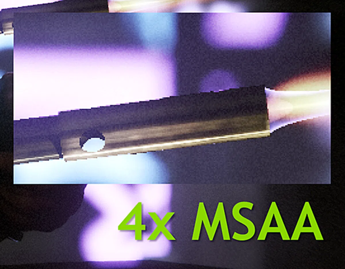
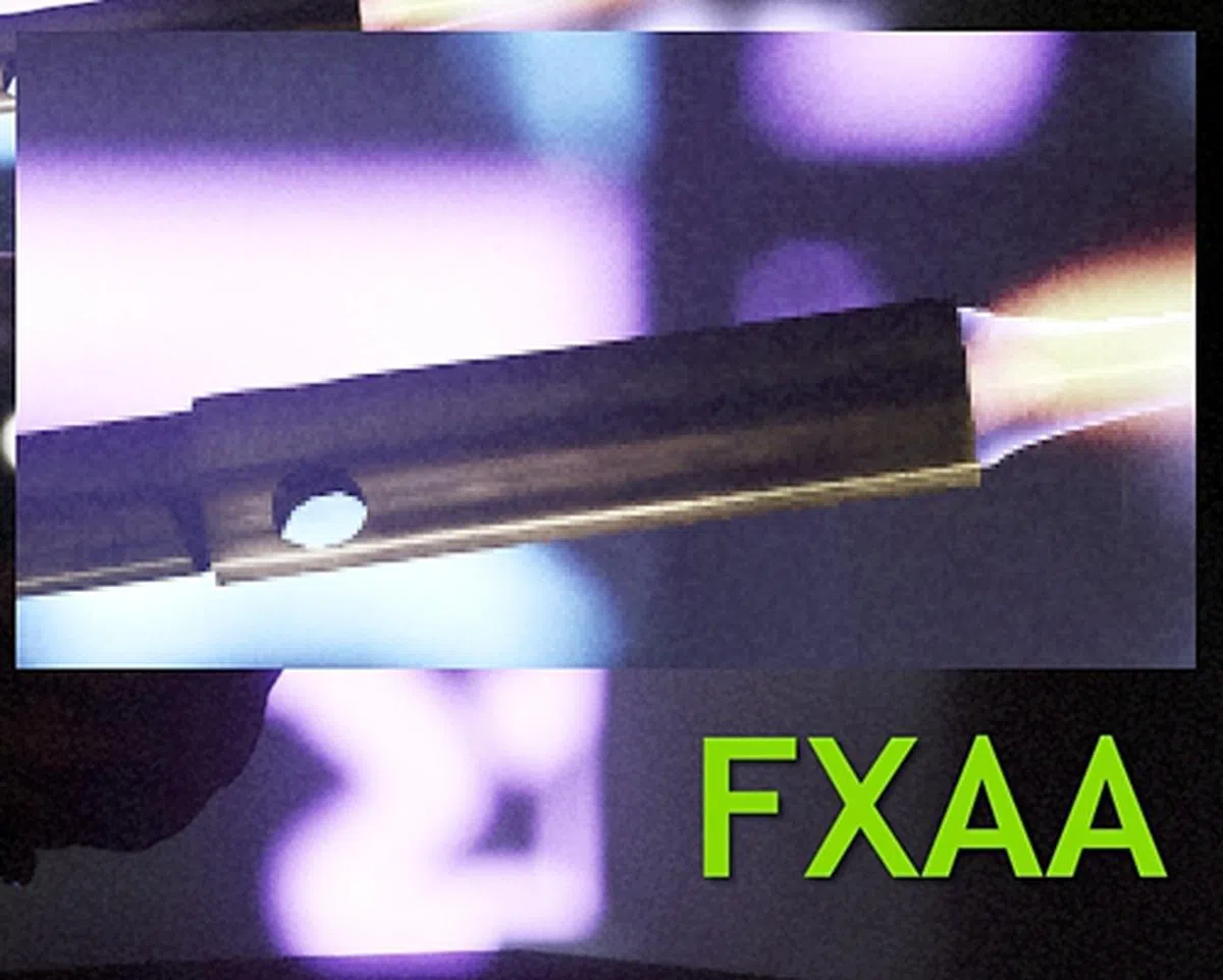
NVIDIA Improves Anti-Aliasing with TXAA
Sometime last year, NVIDIA's FXAA (fast approximate anti-aliasing) algorithm crept into games and offered massive performance gains over traditional multi-sampling anti-aliasing (MSAA). FXAA is actually a post-processing pixel shader program that is able to even run on DX9 compliant hardware and it doesn't require DirectCompute capable stream processors. Working on pixels on the final rendered scene instead of identifying polygons and line edges of other anti-aliasing techniques, FXAA attempts to analyze how much contrast there is between the brightest and darkest pixels nearby to determine the edges. Because of it simplicity, it is fast and used far less memory footprint and in general, a better alternative to MSAA.
For the new drivers with Keppler hardware, such as the GTX 680, FXAA is no longer a game-only option as the driver control panel will now allow you to enable FXAA to enjoy fast and efficient anti-aliasing on any game.
 |  |
TXAA - Topping Off FXAA
It seems like an act of not resting on one's laurel's as NVIDIA seems to have put that saying in action by introducing TXAA. It is touted to be a new film-style anti-aliasing technique that is designed to make use the high texture performance of Kepler's improved Polymorph Engine. TXAA is a technology that is based on hardware anti-aliasing (AA) and software-based (Hollywood-style CG rendering) AA resolve. TXAA offers two modes and they are as shown:-

TXAA has two modes: TXAA 1 and TXAA 2. Both will offer far better quality than 8x MSAA but without the massive performance overhead.
According to the quality versus performance graph shared by NVIDIA, TXAA 1 offers better image quality than 8x MSAA with the game performance equivalent to enabling just 2x MSAA. While that sounds fantastic, TXAA 2 offers even far better image quality than TXAA 1, but with performance comparable to enabling standard 4x MSAA.
TXAA will be first supported on Keppler based hardware like the GeForce GTX 680, but will soon be supported on Fermi class graphics cards such as GeForce GTX 400 and 500 series of graphics cards through driver updates. Games supporting TXAA will be released later this year, but we hope it will one day be a driver settings option for users to enjoy across all games.
Adaptive VSync
Besides smoothing over the jagged effects of aliasing, NVIDIA is attempting to tackle the visual effect of artifacts tearing with its adaptive VSync technology. Tearing occurs due to a mismatch with frame rates of rendered in-game scenes with that of the monitor. NVIDIA has implemented its adaptive VSync technology with its release of their Release 300 drivers that accompany the GeForce GTX 680. Once again, this is yet another feature that NVIDIA will eventually implement in the general driver stack to also enable it on Fermi based cards in time to come.

A pictorial representation of NVIDIA's adaptive VSync technology. It allows for smoothing gameplay by reducing stutter due to mismatch frame rates of game scenes and hardware display.
NIVIDA's adaptive VSync technology works by turning VSync on or off to make the frame display more in rhythm, thus reduces tear/stutter during gameplay. When frame rates drop below 60fps, VSync is disable, allowing frame rates to run unfettered to reduce stuttering. Once the frame rates are above the threshold, VSync is turned on to reduce tearing.
3D Vision Surround on a Single GPU!
GeForce GTX 680 is marketed as capable of supporting 3D Vision Surround on up to three monitors natively on the new GPU due to its new display engine. According to our in-depth interview with NVIDIA engineers, Geforce GTX 680 is actually capable of supporting up to four monitors in 3D; however, the engineers did not see the practical usage of such a multi-display setup. If you think about it, what they say makes sense as the ideal setup comprises of three displays as incorporating a fourth display would prove disruptive for surround gaming purposes, no matter which way you stack those screens.
To prevent the fourth screen support from going to disuse, NVIDIA's drivers allows using a fourth screen for for general computing purposes. NVIDIA labels the fourth and crowning display as an accessory display. It allows the gamer some respite from the 3D Vision Surround visuals provided by the other three displays, to check his Facebook news feed or even his emails!

A lone GeForce GTX 680 supports up to four displays!
Finally, you don't require two NVIDIA GPUs to setup triple displays for 3D gaming and we can't tell you how much a relief this news is going to be for multi-monitor aficionados. From further querying the NVIDIA staff, they mentioned that the native display support for up to four monitors will extend to even the GeForce GT 640M mobile GPU. In essence, we can extrapolate this support to mean that all Keppler based GPUs can handle up to quad displays.
NVIDIA GeForce GTX 680 - Stacking Up Against the Competitors
The reference GeForce GTX 680 card looks vaguely similar to the GeForce GTX 580. Its differences lies skin-deep with its 1536 CUDA cores and eight Polymorph Engines (version 2.0). GeForce GTX 680 also features a GPU fan made from an acoustic dampening material, reducing the noise it emits as it spins to cool the card. The second feature is its heatsink with an improved finstack for better airflow to ensure optimized cooling.The third feature are the triple heatpipes that resemble a pretzel in direct contact with the Kepler GPU for better heat transfer to the heatsink.
Apart from making the GeForce GTX 680 fast and superior to its older series, one of its design goals was to make it the quietest ever top-end graphics card and we believe they succeeded with all the efforts put into the cooler design. For a closed chamber type of cooler, the GeForce GTX 680 was miles ahead of the competition in being quiet, no matter if it was on idle or load throughout our testing,

The finstack of the heatsink that sits beside the GPU fan made from acoustic dampening material. If NVIDIA can pull out such stops for its reference card, we wonder what the card manufacturers would have to do to go above this bar that NVIDIA has set with these features.
Model | NVIDIA GeForce GTX 680 | AMDRadeon HD 7970 | AMDRadeon HD 7950 | NVIDIA GeForce GTX 580 | AMDRadeon HD6970 |
Core Code | GK104 | Tahiti XT | Tahiti Pro | GF110 | Cayman XT |
Transistor Count | 3540 million | 4300 million | 4300 million | 3000 million | 2640 million |
Manufacturing Process | 28nm | 28nm | 28nm | 40nm | 40nm |
Core Clock | 1006MHz | 925MHz | 800MHz | 772MHz | 880MHz |
Stream Processors | 1536 Stream processing units | 2048 Stream processing units | 1792 Stream processing units | 512 Stream processing units | 1536 Stream processing units |
Stream Processor Clock | 1006MHz | 925MHz | 800MHz | 1544MHz | 880MHz |
Texture Mapping Units (TMU) or Texture Filtering (TF) units | 128 | 128 | 112 | 64 | 96 |
Raster Operator units (ROP) | 32 | 32 | 32 | 48 | 32 |
Memory Clock | 6008MHz GDDR5 | 5500MHz GDDR5 | 5000MHz GDDR5 | 4000MHz GDDR5 | 5500MHz GDDR5 |
DDR Memory Bus | 256-bit | 384-bit | 384-bit | 384-bit | 256-bit |
Memory Bandwidth | 192.3GB/s | 264GB/s | 240GB/s | 192.4GB/s | 176GB/s |
PCI Express Interface | PCIe ver 3.0 x16 | PCIe ver 3.0 x16 | PCIe ver 3.0 x16 | PCIe ver 2.0 x16 | PCIe ver 2.0 x16 |
Molex Power Connectors | 2 x 6-pin | 1 x 6-pin, 1 x 8-pin | 2 x 6-pin | 1 x 6-pin, 1 x 8-pin | 1 x 6-pin, 1 x 8-pin |
Multi GPU Technology | SLI | CrossFireX | CrossFireX | SLI | CrossFireX |
DVI Output Support | 2 x Dual-Link | 2 x Dual-Link | 2 x Dual-Link | 2 x Dual-Link | 2 x Dual-Link |
HDMI | 1 | 1 | 1 | 1 (mini-HDMI) | 1 |
DisplayPort | 1(version 1.2) | 2 (version 1.2 HBR2) | 2 (version 1.2 HBR2) | None | 2 (version 1.2) |
HDCP Output Support | Yes | Yes | Yes | Yes | Yes |
Street Price | Launch Price: US$499 | Launch Price:US$549 | ~US$449 | ~US$509 | ~US$349 |

The GeForce GTX 680 has been designed for quieter gaming and when it was under load during our benchmark testing, the GPU fan was visibly quiet even when fan speed was set at 60%. Do refer to our test setup section of the article for more details on the usage of EVGA Precision, a third party utility for tweaking the GTX 680 graphics card.

The card features two Dual-Link DVI ports, a HDMI port and a DisplayPort for support of up to four displays - all natively on the GPU.

The 6-pin power connectors are staggered in position so that the release pins of the power plugs from the PSU are not aligned. This allows for easier removal of the power plugs from the graphics card. However, the design also hints of an even faster GPU variant that could take up yet another power socket with the spare space; time will tell if we're right.
Test Setup
As usual, the following are the specs of our trusty graphics card test bed system:-
- Intel Core i7-975 (3.33GHz)
- Gigabyte GA-EX58-UD4P motherboard
- 3 x 1GB DDR3-1333 G.Skill memory in triple channel mode
- Seagate 7200.10 200GB SATA hard drive
- Windows 7 Ultimate 64-bit
With reference to our earlier article on the AMD Radeon HD 7900 series, we are recalling a smaller sample of cards for comparison against GeForce GTX 680.
The list of cards tested and driver versions used:
- NVIDIA GeForce GTX 680 2GB GDDR5 (ForceWare 300.99)
- AMD Radeon HD 7970 3GB GDDR5 (AMD Catalyst 12.2 Preview Version)
- AMD Radeon HD 7950 3GB GDDR5 (AMD Catalyst 12.2 Preview Version)
- NVIDIA GeForce GTX 580 1560MB GDDR5 (ForceWare 280.26)
- AMD Radeon HD 6970 2GB GDDR5 (AMD Catalyst 11.11)
The list of benchmarks used:
- Futuremark 3DMark 11
- Crysis Warhead
- Far Cry 2
- Crysis 2
- Batman: Arkam City
- Dirt 3
- Unigine v2.1
- S.T.A.L.K.E.R.
EVGA PrecisionX - New Addition to our Test Setup
EVGA PrecisionX is a third party utility we used for tweaking our reference GeForce GTX 680 card. The software is able to access the NVIDIA API directly to adjust the settings of the card. We've used this to monitor our various tested games to allow you to see just how GPU Boost varies from application to another. Additionally, we've also used this tool for our overclocking runs.

The slick and polished interface of EVGA PrecisionX utility software. The sliding bars adjust the Power Target, GPU Offset Clock and Memory Overclock Offset. We shall look at the settings shortly. In summary, this nifty piece of software provides information about the card at a glance and allows power users to tweak hardware settings of the card with relative ease.
Sliders
- Power Target: this will push the card to draw more than its rated TDP of 195W (which is 100% by default). This is strongly recommended for power tweakers only.
- GPU Clock Offset: this slider is targeted at overclockers as it will push up the base clock and the boost clock accordingly.
- Memory Clock Offset: the slider will increase the memory clock speed, though it normally doesn't provide much gain.
Buttons (at least those you should pay attention to)
- Adjust Voltage: click on this button to access the slider controls that allows for over-volting of the card.

Upon clicking the Adjust Voltage button will bring up the EVGA EVTune interface for over-volting the GPU. Its default voltage is 0.987mV and we recommend not pushing it beyond 15% of its default value.
- Monitoring: this button will invoke the 'real-time' monitoring information in their graphical form.
- Performance Log: click this button to reveal the Properties tab that will allow the user to set different aspects of the card the user needs to keep track of.

The Monitoring tab allows the user to select which aspect of the card to monitor. It also allows the user to set the upper and lower bounds of the y-axis of the graphs displayed.
- Frame Rate Target: click this button to reveal the slider to set a target FPS that the card should attempt to reach in order to achieve smoother gameplay. For games that can easily achieve the usually preferred 60fps target, setting the slider to this value would mean that the graphics card can function more efficiently by varying its clock speeds down (and saving power) to provide just the expected performance output.
3DMark 11 Results
We begin our performance analysis with the ubiquitous and widely-used 3DMark 11 benchmark. Here, the new GeForce GTX 680 managed an impressive 8937 3DMarks on the Performance preset, a good 16% more than AMD’s Radeon HD 7970. In fact, its score was almost on a par with the dual-GPU GeForce GTX 590 and it isn’t actually that far off from the dual-GPU Radeon HD 6990’s score of 9116, which is the highest here. Even when looking at the Extreme preset, the GeForce GTX 680 maintained its superiority over the Radeon HD 7970. Clearly, NVIDIA isn’t kidding when they said they’ve built the most powerful GPU ever.

Battlefield Bad Company 2 Results
On Battlefield Bad Company 2, the GeForce GTX 680 once again posted impressive numbers. Overall, the GeForce GTX 680 was easily about 20% faster overall compared to the Radeon HD 7970. And despite the Radeon’s larger frame buffer, even at a resolution of 2560 x 1600 it couldn’t put up a fight against the sheer graphics-crunching horsepower of the GeForce GTX 680. Again, we noticed that the scores of the GeForce GTX 680 wasn’t that far from from the dual-GPU GeForce GTX 590 and Radeon HD 6990.

While running the gaming benchmark, we also fired up the performance log to have a look at the card's real-time performance. The snapshot below was obtained when we ran Battlefield Bad Company 2 with the highest settings used during our benchmark run to ascertain its performance under such load. Ignore the start and ending portions of the graph since those periods correspond to periods prior and after the benchmark routine.
Notice that the GPU core clock speed hits a stable maximum of 1100MHz while its GPU usage hardly lets up at 99% during the duration of the benchmark. Power target level peaks out at 101%. Now that's effective use of the GPU Boost at work and definitely helps the card's performance too as seen from the results above.

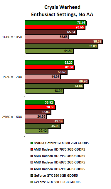
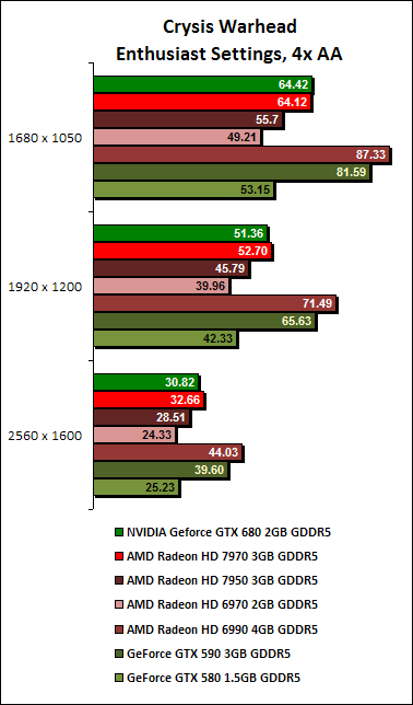
Crysis Warhead Results
On Crysis Warhead, we noted that the Radeon HD 7970 put up a much better fight, seeing that their scores were almost identical. Comparing the GeForce GTX 680 against its predecessor, the GeForce GTX 580, we can see a healthy performance increase of more than 20% across all resolutions and settings.
 |  |
According to the performance log, the GPU clock speed reaches an average of 1084Hz, with power usage at 97% in our example below. At this point, the temperature was 77.0 degrees Celsius. At certain points of the benchmark, the GPU clock reached a maximum of 1100MHz but at that point, its power usage registered 87%, meaning it had some headroom to boost clock speeds and it did just that.

Far Cry 2 Results
On Far Cry 2, the GeForce GTX 680 absolutely blitzes the Radeon HD 7970. With 4x AA enabled, the GeForce GTX 680 was about 15% faster than the Radeon HD 7970. With 8x AA enabled, the GeForce GTX 680 increases its advantage to more than 20%. In fact, on the lower resolutions of 1680 x 1050 and 1920 x 1200 pixels, the GeForce GTX 680 was about on par with the previous generation dual-GPU cards.
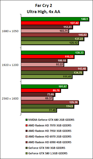 | 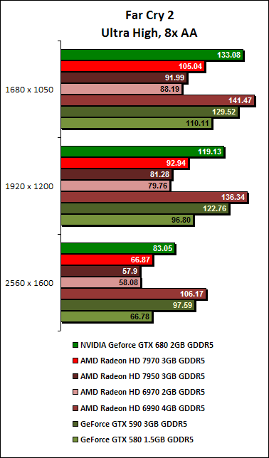 |
For the Far Cry 2 benchmark, the GPU clocks reached a maximum of 1100MHz, with power consumption at 89%. During the duration of the running the benchmark, its GPU temperature was roughly 62 degrees Celsius, cooler than its average temperature recorded for Crysis Warhead. In the graph, you'll notice three distinct segments because we used a benchmarking tool to obtain three consecutive runs in one flow.

Crysis 2 Results
Moving on to Crysis 2, the GeForce GTX 680 continued to outperform the Radeon HD 7970. On the lower resolutions of 1680 x 1050 and 1920 x 1200 pixels, the GeForce GTX 680 was comfortably ahead of the Radeon HD 7970. However, when running at the ultra-high resolution of 2560 x 1600, the Radeon HD 7970 managed to restore some parity, but by then frame rates were already below the playable threshold of 30 fps. Perhaps a larger frame buffer for the GTX 680 would have helped.

For this gaming benchmark, the GPU clock speed reaches an average of 1084Hz, with power consumption at our recorded instance spiking to 107%. Its temperature increment was gradual, from our recorded reading of 57.0°C to its gradual peak at about 61.0°C. At certain points of the benchmark, the GPU clock reached a maximum of 1100MHz but at that point, its power consumption registered just 67%.

Batman: Arkham City Results
On Batman: Arkham City, the GeForce GTX 680 performed stunningly. On a whole, it was more than 15% quicker than the Radeon HD 7970 and was even quicker overall than the dual-GPU GeForce GTX 590 and Radeon HD 6990. Of course, we should also not forget that PhysX that's supported on the card contributed to the score further.

In Batman: Arkham City, the performance log was registering a large portion of GPU activity outside the actual gaming benchmark. The actual benchmark logging began when the power consumption graph was registering its wild swings. The GPU clock had its peak at 1100MHz with seemingly regular troughs at 1006MHz. GPU temperature averaged at about 57.0 degrees Celsius.

Dirt 3 Results
The GeForce GTX 680's impressive performance continued on Dirt 3 where it easily blitzed the Radeon HD 7970 by more than 25%. In fact, it also comfortably thrashed the dual-GPU Radeon HD 6990 and its results were comparable to GeForce GTX 590.

In our final gaming benchmark Dirt3, the GPU clock jumped to its maximum of 1100MHz and stayed there for the duration of the test. The GPU ran at a peak temperature of 66.0 degrees Celsius while power consumption was averaging 98%. So far in our case, GPU Boost was able to get the GPU to run at 1100MHz for the most part of our benchmark tests.

Unigine "Heaven" 2.1
The tesellation performance of Polymorph Engine 2.0, featured in SMX architecture of GeForce GTX 680, is put to the test against the strong contenders from AMD. The Kepler-based card from NVIDIA only managed to pull ahead from the AMD Radeon HD 7900 series at the low and middle resolutions used in our tests. It lost only its lead by a margin of approximately 5% to AMD Radeon HD 7970 at the highest resolution of 2560 x 1600 on the run when the AA settings of Unigine "Heaven" was set at 8x.
Against its own compatriots, the strengths of the GeForce GTX 680's new Polymorph Engine showed as it beat GeForce GTX 580 on all fronts of the tests. Only GeForce GTX 590 is the affirmative king-of-the-hill for the benchmark scores.
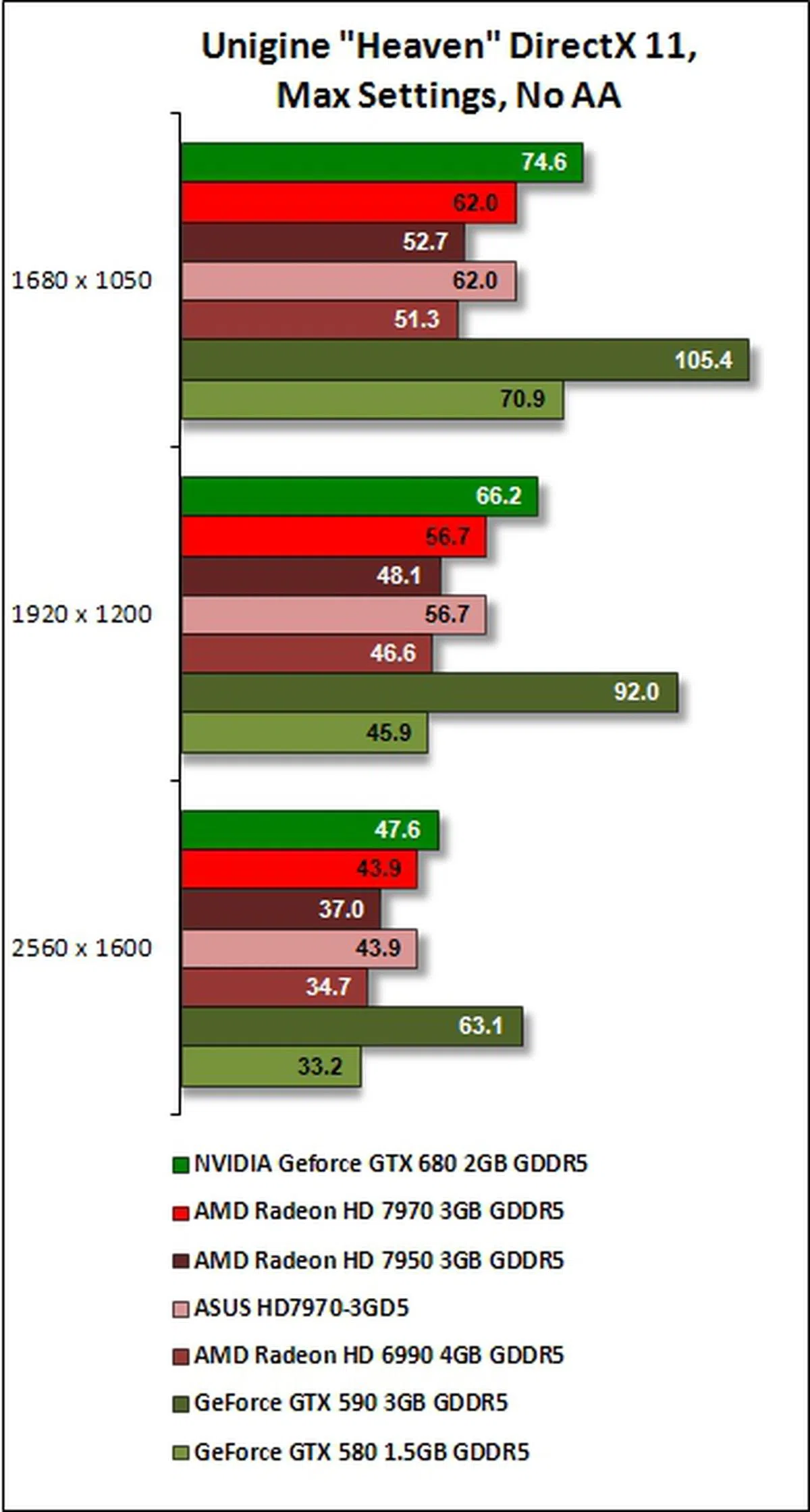 | 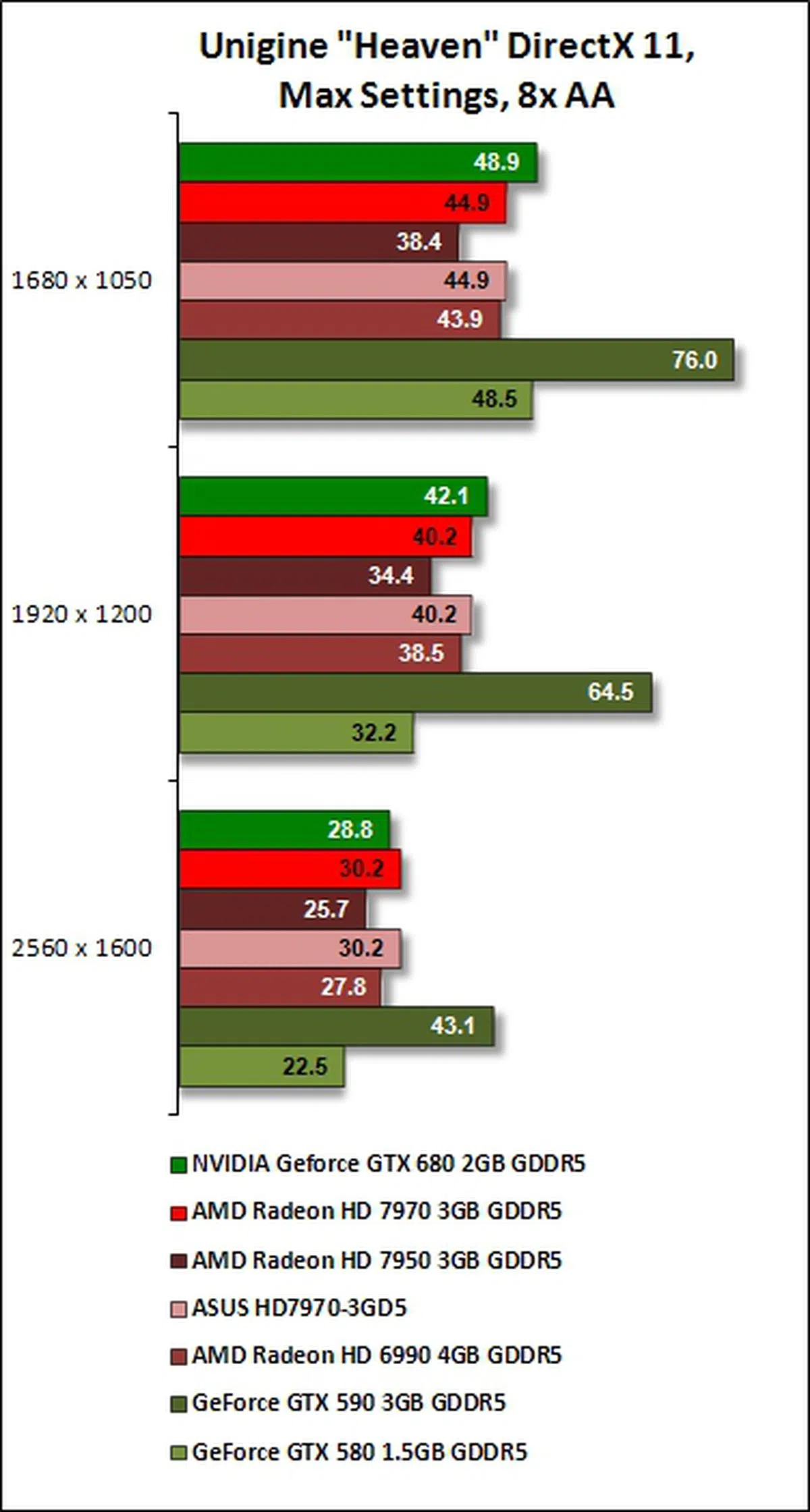 |
The GTX GeForce 680 hits a maximum of 1100MHz for its GPU core clock speed for the duration of the test. It ran at a temperature that hovered around 66 degrees Celsius. We observed a sharp dip in power consumption during the test; however, on the whole, power consumption remained at 92% during load periods. Given its GPU Boost level, we were a little surprised that it didn't really pull ahead of the AMD cards by a notable margin.

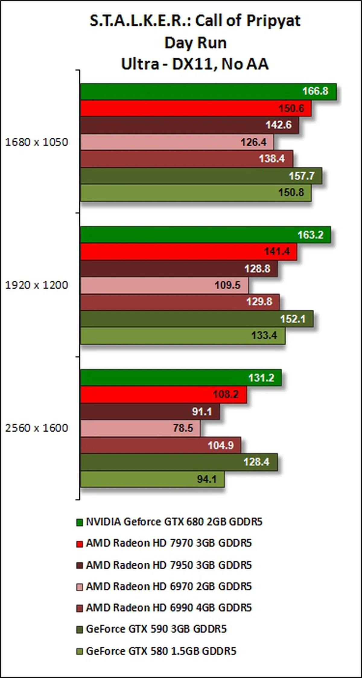
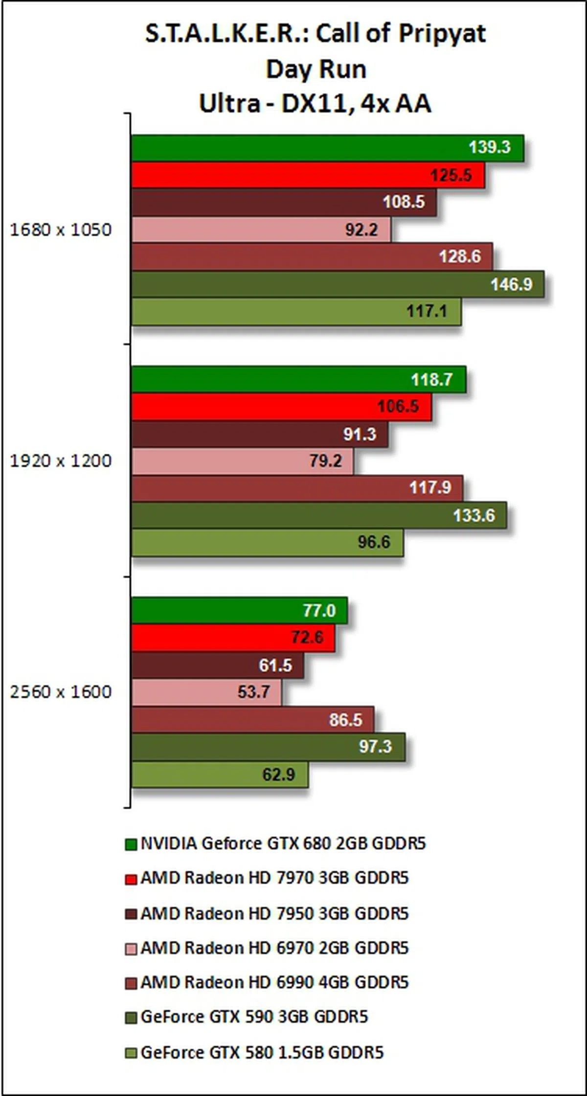
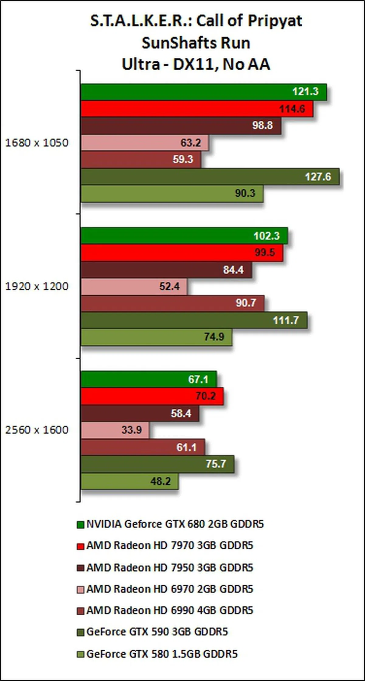
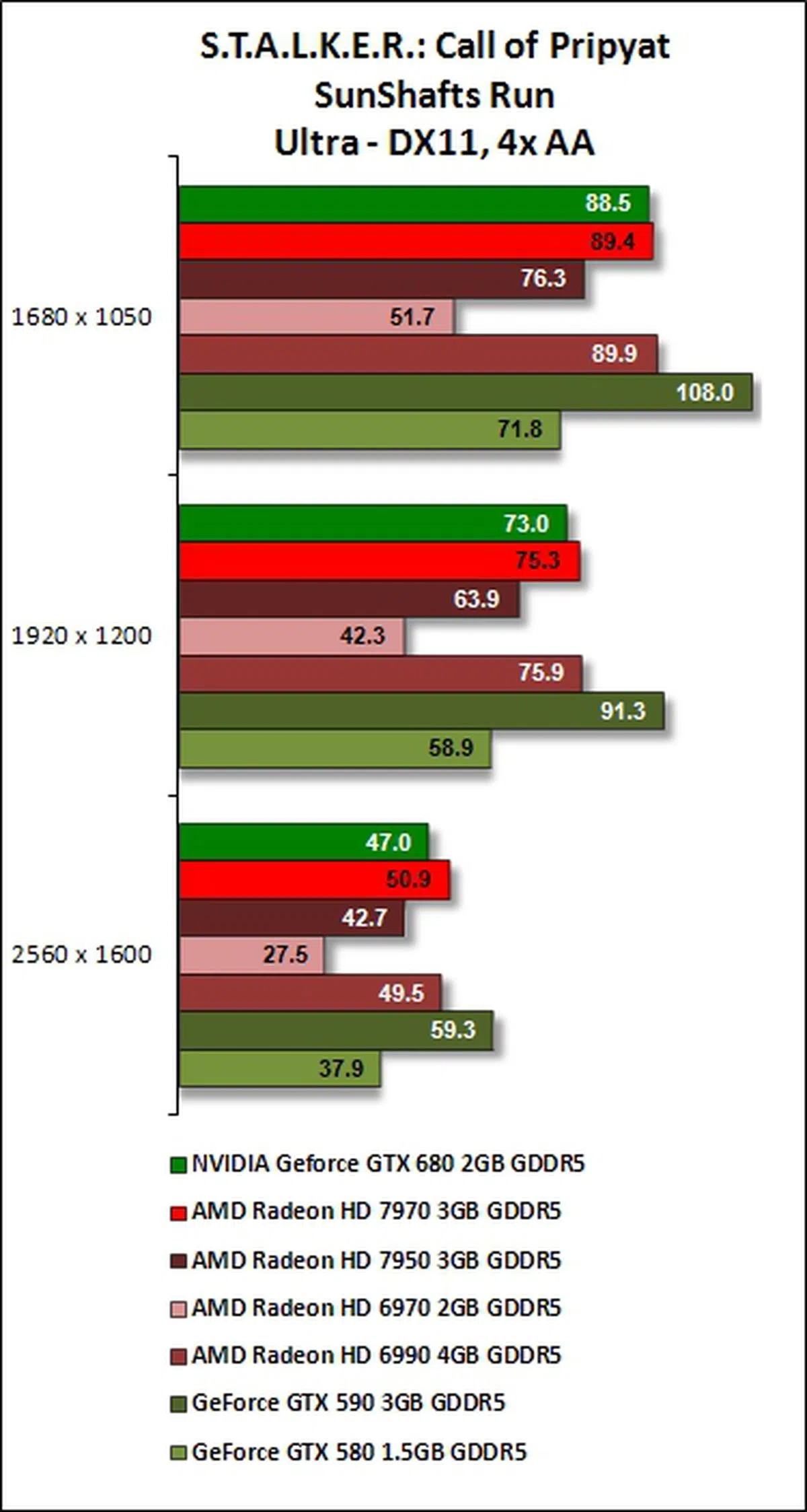
S.T.A.L.K.E.R.: Call of Pripyat Results
Kepler's strong showing in tesellation performance is evident again for this benchmarking test. Compared to Unigine (GTX 680's losing margin was almost 50% against GTX 590 at the benchmark's highest test settings), its performance is better as GeForce GTX 680 narrowed its losing margin to GeForce GTX 590 to about 27% when the benchmark was set at its highest resolution, with 4x AA enabled. At these benchmark settings, the GeForce GTX 680 also met its match when compared against AMD Radeon HD 6990.
For fair comparison, it beat the AMD Radeon HD 7900 series cards on almost all runs of the benchmarking software, taking the shine off their new GCN architecture that was crucial to the relative improvement in their DX11 performance. Only in the SunShafts run with 4x anti-aliasing involved, the Radeon HD 7970 was a wee bit faster than the brand new GeForce GTX 680. Seems like the Radeon cards have really pulled up their DX11 performance and are rivaling NVIDIA.
DirectX 11 Results
 |  |
 |  |
All graphs, from the monitoring logs of Extreme Precision X utility, seem to share a regular rhythmic pattern where you can figure out the pauses in the gaming benchmark to the load periods of it. The card again reaches a maximum of 1100MHz for its GPU clock speed while its power consumption hits an average value of 101% during the run of the benchmark. For the hardcore folks, do remember that you can get more out of the card from overriding its power target, but realistically, it won't go a lot higher than 110% in actual monitoring since the card has its own internal safety limits set in stone.

Temperature
At load conditions, the the card runs at 69 degrees Celsius. This may be attributed to its lower power consumption (195W TDP) as well as its new finstack of its heatsink. We wonder if the third party card manufacturers would be able to lower the temperature bar further as they roll out their variants of the GeForce GTX 680 in the near future. Compared to the GTX 580, it's a marked improvement.

Power Consumption
The GeForce GTX 680 has the third lowest power consumption and it was not as power efficient as AMD Radeon HD 7970 nor, the 7950 even though the new card has a lower TDP rating than the former. One reason for this outcome is due to the GPU Boost working in the background that is always trying to maximize the power budget of the GPU where possible. This means it is better utilized than other graphics cards of the past and as a result of its higher performance, you pay somewhat in its power consumption. At least it's much more efficient than the last generation of products. Overall, given its performance aspects, we think the power consumed is reasonable.

Overclocking
For our overclocking efforts, we made use of EVGA Precison X utility software. We managed to push the GPU Clock Offset slider to a value of 130MHz. For its memory subsystem, we managed to garner a headroom of 300MHz. For these settings, we left the voltage of the card at its default value of 0.987mV. NVIDIA GeForce GTX 680 managed to blaze ahead of the dual-GPU cards, besting AMD Radeon HD 6990 by a margin of approximately 4.4% at Performance settings! The other cards were trailing in its wake. At Extreme settings, GeForce GTX 680 was beaten by AMD Radeon HD 6990 by a margin of 3.6%. A close call indeed.

In order to ascertain the nett GPU clock speed we have achieved from our overclocking efforts, we ran the performance monitoring tools in the background. We managed to reach a GPU clock speed of 1240MHz with our GPU Clock Offset set at 130MHz. This meant that we managed to increase the default boost clock of 1058MHz by approximately 17% and we saw a GPU Boost of 9% in action when you consider the new base clock of 1136MHz (which is 1006 + 130).

The Over-Volting Attempt
In our attempt to achieve higher GPU Clock Offset margins, we over-volt the card's GPU to 1.100mV. This allowed us to set the GPU Clock Offset margin by a slight gain of 4MHz to 134MHz with the its Memory Clock Offset at the same headroom level of 300MHz. Our performance took a dip at both settings of 3DMark11, with its Performance score registering at 9121 (a reduction of 4.2% against its earlier score of 9513); while its Extreme settings score was whittled down by a margin of 3.2% to 3150. While your experience may vary, it looks like our advice is to forget about over-volting the card.

Peering into the monitoring graph, we understood better as to why our over-volting attempt didn't go well. Though we managed to increase the card's GPU Clock Offset by a meagre 4MHz to 134MHz, the highest recorded core clock speed was 1154MHz! This was about 7.5% lower than what we had achieved without increasing the operating voltage of the card.

Kepler's Laws Are Binding and Enforced
With the GeForce GTX 680 labeled as its new flagship product based on the Kepler architectures, we feel that NVIDIA has posed a serious challenge to AMD even though the latter has had a head-start in bringing its Southern Island GPUs to the retail market. The first and probably most significant guiding principle of achieving higher clock speeds with its Kepler GPU core has entailed in the evolution of its previous generation streaming multiprocessor (SM) block to Kepler's current updated SMX block. Besides sporting a re-jigged architecture, the launch of Kepler marks the adoption of the 28nm silicon fabrication process for its new generation GPUs. Its adoption also allowed Kepler to pack in many more CUDA cores into each SM block and yet managed twice the performance per watt of the old SM block. As a result, GeForce GTX 680 takes the pole position as the fastest single-GPU graphics card now - in most cases at least.

Putting the GeForce GTX 680 through its paces, we found it a serious challenge to AMD's Radeon HD 7900 series GPUs. In our earlier review, we wondered just how long AMD would be able to keep its first-to-market advantage. Now, we know for certain that AMD has met its match with the launch of Kepler's new architecture. And if we're right, the green camp could have something even faster than the GeForce GTX 680 in the months ahead.
Not only is GeForce GTX 680 taking the lead in most of the benchmark tests, its suggested pricing of US$499 puts its squarely between AMD Radeon HD 7970 and 7950. If the launch price holds true, AMD will need to reduce its pricing of its two 7900 series variants in order to hold on to what little first-to-market advantage it has had enjoyed till now.
The Kepler GPU has also achieved its mark with lower power usage and NVIDIA has in-turn used its balance power consumption overhead to boost GPU clock speeds for further performance. Called GPU Boost, it works well as we've seen from our testing. The concept is very similar to Intel's Turbo Boost to maximize performance from the silicon. As such, our standard power consumption test isn't quite as reflective of its capabilities because the GTX 680 is trying to boost its clock speeds to use up balance power budget while the comparison GPUs function normally. In any case, we feel that NVIDIA deserves a mention here for its efforts in balancing power efficiency with GPU performance. Its superlatives don't just end there as it's also the quietest high-end graphics card ever - no matter at idle or at load.
With its performance, power efficiency, quiet operation and a list of new distinguishing features, the GeForce GTX 680 is easily a GPU which we will strongly recommend for your gaming needs. With its improvement over the previous generation for 3D Vision Surround on just a single GPU (and even supports a fourth screen for miscellaneous usage), Kepler further consolidated its lead as the choice graphics card for gamers who need to satisfy their 3D gaming needs. For a single-GPU graphics card, the GeForce GTX 680 is quite a remarkable one when considering all of its improvements and capabilities.
What's next now? Well, if you consider the GeForce GTX 680's GK104 core code, it's meager 195W TDP, a spare spot for yet another power connector, the interesting price point and the rumors of a faster GPU SKU, all these signs seem to point that NVIDIA does have something else in the works that would easily exceed the GTX 680. Of course at this juncture, NVIDIA doesn't really have an urgent need to reveal anything else superior but we've a strong hunch that they are saving the cream of the crop for a later time. Nevertheless, expect to see the Keppler architecture trickle down the series to many other price points in the months ahead, including refreshing the mobile GPU lineup like the GeForce GT 640M that is featured in the slimmest and lightest multimedia machine ever, the Acer Aspire Ultra M3.
Our articles may contain affiliate links. If you buy through these links, we may earn a small commission.