
High-End Intel Z87 Motherboard Shootout
The launch of the 4th generation Intel Core processors brought with it a new LGA 1150 CPU socket and the Intel 8-series motherboards. We rounded up the top-end Intel Z87-based motherboards from five manufacturers (ASRock, ASUS, ECS, Gigabyte, MSI) and put them through their paces. Find out who came out on top!
Introduction
In June last year, Intel launched their 4th generation Intel Core processors that are also popularly referred to by their codename "Intel Haswell". We understand that some sharp observers have questioned the exact changes behind Haswell's CPU microarchitecture as it is still based on the same 22nm process technology with 3D Tri-Gate transistors as that used on the previous generation "Ivy Bridge" processors.

The Intel Core i7-4770K processor boasts of an updated microarchitecture that brings about better power efficiency. It also has an updated Intel HD 4600 graphics core that enough features and firepower to put all entry-level discrete graphics cards out of business.
Actually, the major improvement brought about by the Haswell processor is the improved graphics engine core. The top-end Intel Iris Pro Graphics 5200 graphics core engine is currently exclusive to Intel Haswell mobile and non-socketed desktop SKUs; however, this will change in the near future with the impending arrival of the 14nm Intel Broadwell processors. From our review of the performance of the integrated graphics engine (Intel HD Graphics 4600) of the Intel Core i7-4770K CPU, we found that there were marked improvements over the previous generation Ivy Bridge processors' IGPs. Hence, it is ideal for system builders looking to build a mid-range desktop system without the need for a discrete graphics card (depending on the processor chosen). Also, the new graphics engine's API support has been expanded to include Direct X 11.1.
In addition to graphical compute performance, the other important improvement pertains to power efficiency due to several small enhancements made by the updated Haswell microarchitecture. The CPU voltage regulation phase, which was traditionally handled by the motherboard, has been integrated into the Haswell CPU. This allows for more fine-tuning of the power management aspects of the processor. This feature is actually more to the advantage for mobile Haswell CPUs as the top-end Intel Core i7-4770K desktop Haswell CPU is rated at 84W, which is 7W higher than the Core i7-3770K (Ivy Bridge), possibly due to the more advanced graphics engine.
However, the desktop Haswell CPUs do bring with them a new LGA 1150 socket and the Intel 8-series chipset. In the following section, we will take a quick look at the different chipsets that make up Intel 8-series, and in particular, the Intel Z87 chipset.
Making Sense of the Intel 8-Series Family
The Intel 8-series is made up of the Z87, H87, and H81 Express. There are also the Q87, Q85, B85 Express chipsets that are meant for corporate desktop systems. For end-users, the Intel Z87 Express chipset is the only one in the entire range that will allow you full access to the overclocking features of the K-series Haswell CPUs. However, power users may be let down by the fact that the interconnectivity between the CPU and the chipset is still powered by DMI 2.0. This has remained unchanged over the last two mainstream desktop platforms that Intel had brought to us (these are the Intel Z68 and Z77 Express chipsets).

The block diagram of the Intel Z87 Express chipset.
Like the previous generation Intel Z77 chipset, the Z87 has native support for PCIe 3.0 that translates to more bandwidth for expansion cards, primarily graphics cards. Thus, the Z87 chipset offers support both AMD CrossFire and NVIDIA SLI multi-GPU configurations. This is a result of dividing the 16 PCIe lanes from CPU among the corresponding PCIe 3.0 slots. An improvement is its support for I/O port flexibility that allows some I/O ports to be finalized at the time of design. This means board manufacturers are able to decide which of these ports can be configured as USB 3.0, PCIe, or SATA 6Gbps, allowing manufacturers to have better product differentiation for their different SKUs.
The Z87 chipset supports up to six native USB 3.0 ports and six SATA 6Gbps connectors. The H87 and H81 variants can be considered as mainstream chipsets, intended for the average user. The former is very similar to the top-end Z87; however, it lacks support for CPU overclocking. It also officially supports only up to two graphics cards (plenty enough for most users). The H81 chipset is suitable for small form factor systems as it only supports a single discrete graphics card. It is also has limited support for SATA 6Gbps and USB 3.0; it only drives up to maximum of two SATA 6Gbps devices, and two USB 3.0 ports.
Faced with a rather uninspiring selection of Haswell desktop socketed CPUs, the motherboard manufacturers have to pull out different tricks in order to differentiate their Intel 8-series wares. For starters, despite the official lack of support for unlocked K-series Haswell processor, some board makers like ASUS and MSI who are offering ther versions mainstream H87 boards that will allow system builders to overclock their processors; however, these boards don't support NVIDIA SLI configurations. Therefore, only AMD CrossFireX setups are officially supported by the H87 boards. As such, the Intel Z87 boards are highly recommended for power users and hardcore gamers.
With that in mind, we move ahead with our round-up of five top-of-the-line Intel Z87 motherboards from ASUS, ASRock, ECS, Gigabyte and MSI. Of the five boards, we've featured three of them in a video preview last year, so check it out to get acquainted with them quickly:-

Take note that this article is an extended version of the motherboard shootout article which was published in February 2014 edition of HWM (the sister publication of HardwareZone). As such, actual testing of these boards were done late in 2013.
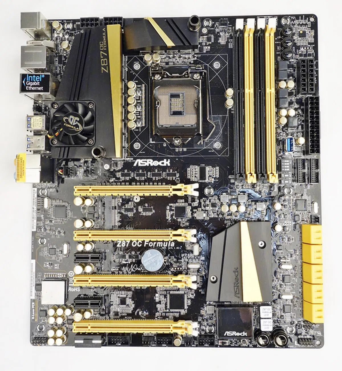
ASRock Z87 OC Formula
The ASRock Z87 OC Formula is touted as a board built for overclocking, with its reliable power design system that features both air and liquid cooling options. At first glance, the board bears a strong semblance to the previous generation ASRock Z77 OC Formula as they both hail from the overclocking series of their motherboard offerings. It is obvious the board is targeted at overclockers and power users.

The ASRock Z87 OC Formula is the only EATX board in our lineup. It sports a slightly wider girth than an ATX board, and true to its OC Formula pedigree, it features the OC Formula Power Kit that drives its 12-phase power delivery system.
With its 12-phase power design system that consists of premium alloy chokes, multi-stacked MOSFETs, and multiple filter capacitors, the board’s digital pulse wave modulation system takes rein to ensure stable power supply to the CPU and memory modules. We also see a pair of barb fittings to support liquid cooling systems for additional cooling of the board's MOSFETs. Speaking of cooling, there is a 40mm intake fan, nested in one section of its VRM heatsinks. The heatsinks are distinctively colored yellow-on-black, with gilded capacitors in front of it that add a nice touch to its finishing.

Seen here are some of the VRM components that make up the OC Formula Power Kit system. We can also see the barb fittings, so that a liquid cooling system can be attached to the VRM heatsinks for the additional cooling.
Near the VRM heatsink, there are two ATX 12V power connectors, instead of one. This is sure to delight overclockers who want to push their unlocked Haswell processors with more power.

There are a pair of ATX 12V connectors. While this is a bonus for those hoping to push the board and their CPU to greater overclocking heights, fortunately it's not mandatory to pair the board with a PSU that has dual 8-pin 12V ATX power connectors.
Moving down south away from the board's LGA 1150 socket, we see a total of four PCIe x16 physical expansion slots. The board is able to support multi-GPU configurations; 4-way arrangements of NVIDIA SLI and AMD CrossFireX technologies are possible with this ASRock board. The top PCIe Gen 3.0 x16 slot operates at x16 mode when only one PCIe Gen 3.0-compilant graphics card is installed. If the second slot is occupied in a two card setup, the 16 PCIe lanes would be even split between the two occupied PEG slots; with each slot allocated the bandwidth of 8 lanes. In a 3-way setup, the lane configuration would be in this manner, x8/x4/x4, as the eight lanes from the second slot has to be shared with the third slot. In the event, the avid gamer maxes out all the four x16 slots, the embedded PLX PEX8608 eight-lane PCIe 2.0 switch will come into play by allocating four PCIe 2.0 lanes (supplied by the chipset) to the last slot, with a final lane configuration of x8/x4/x4/x4 to support a 4-way graphics card configuration. Other expansion slots include a pair of PCIe 2.0 x1 slots. Also, nested between the first two PCIe Gen 3.0 x16 slots is the mini-PCIe slot. This slot is shared with the second PCIe 2.0 x1 slot.

There are a total of four length PCIe expansion slots that allows the board to support up to four graphics cards.
Additional power to drive such a graphical setup with stability comes courtesy of a SLI/XFire power connector that is located near the bottom edge of the board.

The SLI/XFire power connector that will deliver more power in a multi-GPU configuration.
Another notable feature is the Purity Sound technology that features an on-board Realtek ALC1150 audio codec, complete with EMI shielding to minimize distortion due to electrical interference. Together with the accompanying TI NE 5532 amplifiers, this on-board audio system is touted to provide high quality aural experience.

The Purity Sound system of the board. It's a combination of the Realtek ALC1150 audio codec with TI NE 5532 amplifiers and EMI shielding coming to play.
Besides sporting such pedigree components, the board also boasts of some truly unique features, like its conformal coating that acts as a water repellant for the board's components. This is important for protection against condensation or any spillage or leakage from a closed liquid cooling system. Besides this water proofing feature, the ASRock board's PCB is made up of eight layers that contains 4x 2oz copper inner layers. These copper layers are supposedly able to lower operating temperatures, and promote higher energy efficiency. There is even a little cut-away window next the EMF shield of the Purity Sound, to show the eight layers of the PCB.
Moving along the bottom edge of the board, we see the OLED display that replaces the traditional LED segmented ones. The new display is able to show system status information like operating temperatures, on top of the usual debug codes.

The new OLED status display is highlighted with a red frame. It can display system status information, as well as the usual debug codes.
The ASRock board is built for an open bench work environment as there are a pair of buttons for power and resetting the system. Below the OLED display, there is a switch that toggles between two sets of BIOSes, and there is a button for clearing CMOS, next to the BIOS switch. The headers of at the bottom edge consists of a COM port header (to the right of the SLI/XFire power connector), two chassis fans headers, and a pair of USB 2.0 ones. At the extreme ends, we see a front panel audio header on the left; while on the right, just next to the power button, there is system panel header. It's apparent that due to space constraints, the chassis speaker and power LED headers have been shifted slightly north, nearer to the stack of yellow SATA 6Gbps connectors.
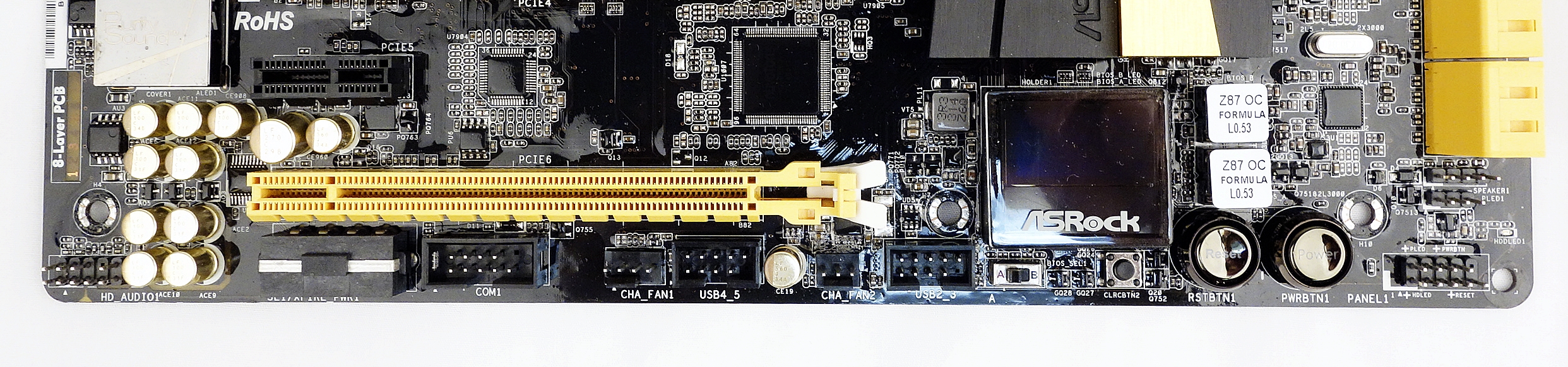
The headers of at the bottom edge consists of COM port header (to the right of the SLI/XFire power connector), two chassis fans headers, and a pair of USB 2.0 headers. At the extreme ends, we see a front panel audio header on the left; while on the right, just next to the power button, there is system panel header. The chassis speaker and power LED headers have been shifted slightly north, near to the stack of yellow SATA 6Gbps connectors.
Although the SATA connectors are all yellow, they are clearly labelled, and we can see the four from the left are driven by the ASMedia ASM1061 controllers; while the remaining six are connected to the Intel Z87 chipset.

The SATA 6Gbps connectors are clearly labelled.
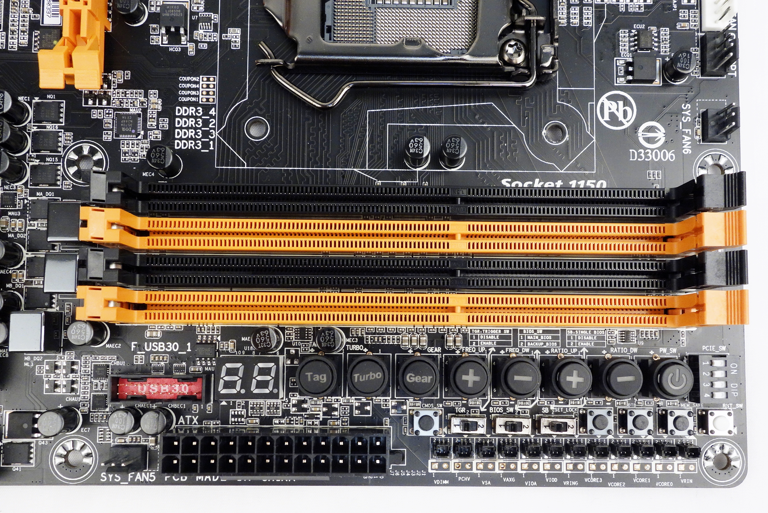
Moving beyond the SATA connectors, right back next to the LGA1150 socket, we see the four DIMM slots that support DDR3 memory modules that have been rated to operate at 3000MHz+, up to a maximum capacity of 32GB. To reiterate the point of the ASRock board being built for an open workbench environment, there are a slew of onboard switches, buttons, connectors and voltage points in the vicinity of the memory slots.

The DIMM slots support DDR3 memory modules that have been rated to operated at 3000MHz+, up to a maximum capacity of 32GB.
Just right next to the yellow DIMM slot, we see three DIP switches. From the left, there is the PCIe On/Off switch that allows you to disable the installed expansion cards without having to remove them from their corresponding PCe x16 physical slots. The other two, single DIP switches useful during LN2 cooling situations; the first one, from left, enables the slow mode feature, and allows the processor to start at a lower clockspeed. The second switch toggles the LN2 mode and is used to overcome the cold-boot bug issues of certain LGA1150 CPUs. Next, we also see the onboard buttons for the Rapid OC feature, allowing you to adjust the the CPU ratio, base clock frequency and the CPU VCore voltage for overclocking.

These onboard features are ideal for an overclocker in an open workbench environment. There is the Rapid OC feature, V-Probe, and the DIP switches for the PCIe x16 slots, and for LN2 cooling setups.
Although the Menu button is right next to the "-" button, the former isn't part of the Rapid OC feature. Instead, it is used to toggle among the date, time, temperature and voltage information for the OLED display that is located at the bottom of the board. Last of all, diagonally to the right of the Menu button there is the V-Probe feature. It is a set of 7 detection points that allows for direct voltage measurements of different motherboard components, including the DRAM, CPU System Agent, chipset core and CPU core.
Finally, moving to the rear I/O ports of the board, we see the now ubiquitous PS/2 keyboard-mouse port that sits below a pair of black USB 2.0 ports. To its right, there is a HDMI-In port, and the HDMI-Out port is below the pair of blue USB 3.0 ports. The clear CMOS button is neatly tucked away among the stack of USB 3.0 ports. For its audio options, the ASRock board has the usual five analog jacks, and a S/PDIF out port.

The I/O panel at the rear of the ASRock board.
*Note: The contents of this page are mirrored over from our initial first looks article of the board. If you've read it previously, you may move on to the next page.
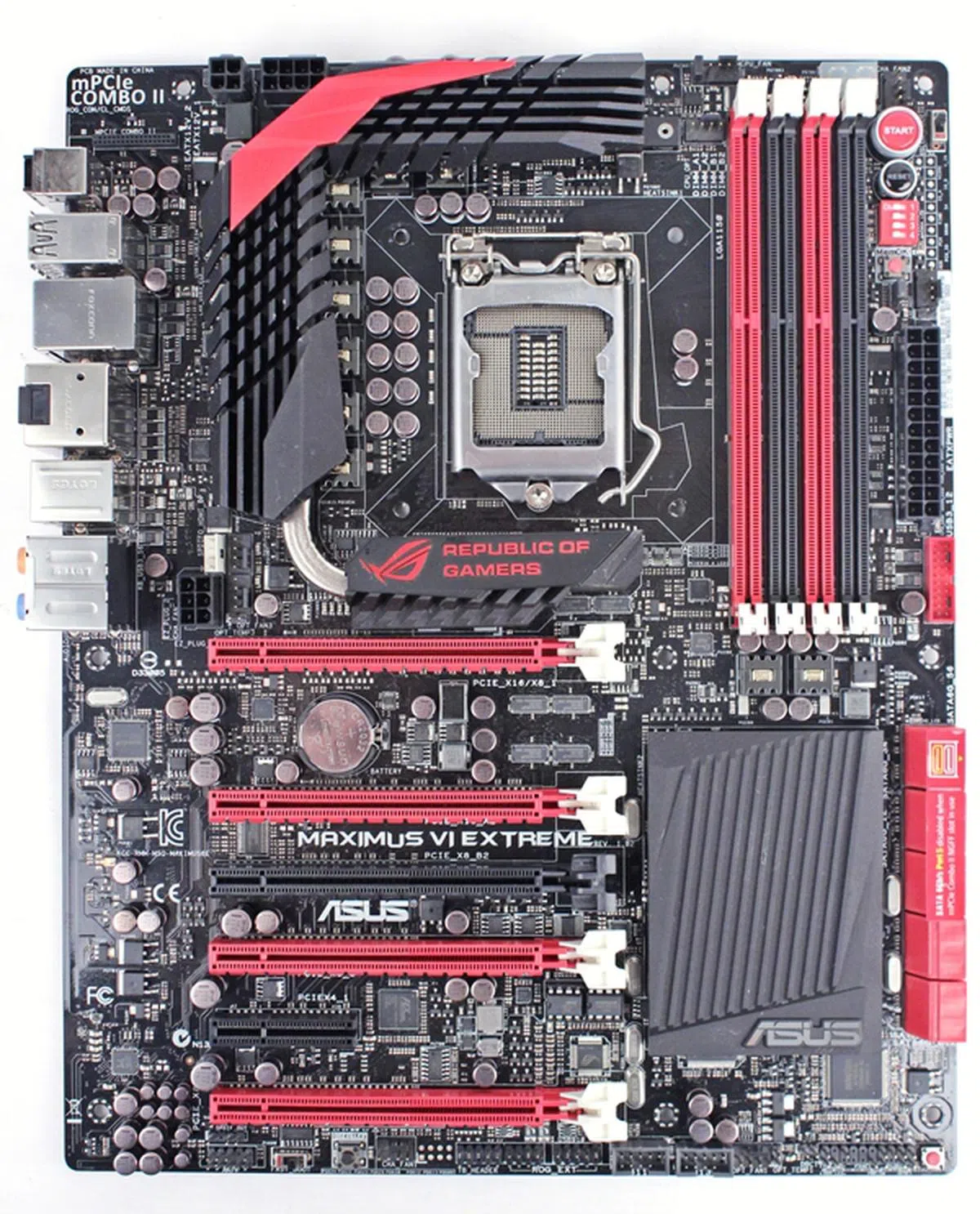
ASUS Maximus VI Extreme
The ASUS Maximus VI Extreme is the flagship Intel Z87 ATX motherboard from its Intel 8-series offerings that we've initially witnessed from the company's technical seminar that we attended a couple of months back. It comes packed with features that will make its target audience of overclockers and power users a really happy bunch. The board sports the familiar red-and-black color scheme of the Republic of Gamers (ROG) series. Featuring the Intel Z87 chipset together with its LGA1150 CPU socket, the board supports the new 4th generation of Intel Core i3/i5/i7 processors. Owners of the previous generation 'Ivy Bridge' CPUs need not apply.

The ASUS Maximus VI Extreme is the flagship Intel Z87 motherboard that is targeted at overclockers and power users. Besides having an upgraded 8 + 2 phase power delivery system for the CPU and memory, the board comes bundled with its exclusive OC Panel for real-time overclocking and system monitoring.
One of its defining features is its exclusive bundled OC Panel. It is a highly evolved version of the OC Key that was first unveiled with the ASUS Rampage IV Extreme Intel X79-based motherboard. The OC Key is a piece of equipment that sits in-between your graphics card and display monitor. Using on-screen display (OSD) technology to control and monitor overclocking and basic BIOS matters, the OC Key attaches a transparent, graphical overlay on the original screen output and provides an informative menu to enable OSD TweakIt and OSD Monitor.

The new OC Panel console that is bundled with the board. On the right, we see the console in its Extreme Mode, with its front cover removed, where overclockers can make use of the onboard headers, switches and temperature probes for hardcore system tweaking.

The OC Panel console is connected to the motherboard with custom data cable, while a SATA power connector is used to power up the console. So if the OC Panel isn't mounted in the 5.25-inch drive bay, it would only be useful and accessible if the system was left in the open. Otherwise you would have to open the casing's side panel to hook up the OC Panel before usage.
The new OC Panel is a complete revamp of the former, and packages real-time monitoring and overclocking capabilities into a sleek, transformable console. The OC Panel can be likened to a customized Fluke digital multimeter, except that this is a gear that's made to handle overclocking and monitoring status. It has two modes of operation. In normal mode, the OC Panel can be installed, with an additional bracket attachment, into a spare 5.25-inch drive bay. According to ASUS, it is excellent for normal overclocking to get that additional performance boost during gaming.

The OC Panel console's screen can be tilted such that the entire console can be slotted into a metal bracket. Following which, the bracket can be secured inside a spare 5.25-inch drive bay of a PC chassis.
On the other hand, while in its Extreme Mode, the same overclocking panel will allow for overclocking with more finesse. Its features include the following:
- VGA SMB
- VGA Hotwire
- Four 4-pin fan headers
- Slow Mode (more on this below)
- Pause Switch
- Multiple Parameter Tuning
According to ASUS, the settings are adjustable in real-time, through the buttons located above the Extreme Mode panel.

The different extreme overclocking settings can be adjusted in real-time from the control buttons located above.

If you plan to keep the OC Panel handy next to you, you can prop it up in this manner.
Crucial to stable overclocking efforts is the board's power delivery system where the ASUS Maximus VI Extreme board features NexFET MOSFETs, BlackWing chokes, and 10K black metallic capacitors that make up its digital Voltage Regulator Module (VRM). The VRM delivers an 8-phase power supply to the CPU; while the memory modules are fed a 2-phase one.

The 10K black metallic capacitors are seated in front of the 60A Blackwing chokes, and the NexFET MOSFETs are covered by the massive heatsinks.
In terms of memory support, the board supports up to four DDR3 memory modules that have been rated to operate at the frequency of 2800MHz while the maximum supported installed capacity is 32GB.

The Blackwing chokes and the 10K black metallic capacitors, highlighted by the red frame, form part of the power delivery system for the DIMM slots.
Near the vicinity of the memory DIMM slots, you will find that ASUS has squeezed in a number onboard features and they consist of the following:-
- Start and Reset buttons
- PCIe x16 DIP switch
This switch allows the user to disable and enable the corresponding PCIe x16 slots. - MemOK! button
This button is useful for overcoming memory module compatibility issues. - Slow Mode switch
This is used when the system is cooled with a liquid nitrogen system. At such low temperatures, the system is switched to slow mode to prevent crashing.
- ROG ProbeIt
Like most other recent ROG boards, this board also features a set of detection points that allow for multimeter voltage measurements for various parameters.

The PCB area near the DIMM slots is choke full of onboard features. The ROG ProbeIt voltage detection points are located below the Slow Mode on/off switch.
More Features
The new Intel Z87 chipset supports up to six SATA 6Gbps ports, against just two that is supported by the previous generation Intel Z77 chipset. Just beyond the DIMM slots, the middle front portion of the board bunched all the onboard SATA connectors.The first six connectors, from the right, are powered by the Intel Z87 Platform Control Hub (PCH); while the four SATA connectors, from the left, are courtesy of the third-party ASMedia ASM106x SATA 6Gbps controllers. While it's great to know that there are no SATA 3Gbps ports and all of them are the 6Gbps variety, we would have preferred the connectors to be color-coded to tell which controller is powering them at one glance.

There is no way to tell the different SATA 6Gbps connectors apart as they are of the same color. Fortunately, there are no SATA 3Gbps connectors present.
Making Sense of the PEG Slots
The board sports a total of five PCIe x16 slots; four of them colored in red and a single black one. At first glance, we thought the PEG configuration was the same as the previous generation Intel Z77-based Gigabyte GA-Z77X-UP7 motherboard we reviewed in March this year, where the black PCIe x16 slot will provide direct connection to the CPU and bypasses the PLX 8747 splitter chip for a true single graphics card configuration. However, this is not the case for the ASUS Maximus VI Extreme. Its single black PCIe x16 slot operates at x8 speed. Its four red PCIe x16 slots support 4-way NVIDIA SLI or AMD CrossFireX graphics setup.

With reference to the photograph above, the red PEG slots, from top to bottom, are labelled PCIE_X16/X8_1, PCIE_X16_A2, PCIE_X8_3, and PCIE_X8_4. As you can decipher, each slot has its best possible configuration labelled. Bearing that in mind, onboard the Maximus VI Extreme there's a high-end PLX PEX 8747 high speed switching chip takes in the 16 PCIe lanes from the PCIe 3.0 controller of the 4th generation Intel Core CPU, and serves out a total equivalent of 32 PCIe lanes. The PLX PEX 8747 is effectively a 5-port, 48-lane high-speed switch and supports the following configurations:-

The common port configurations of the PLX PEX 8748 switch. (Image Source: PLX Technology)
As a result, the board is able to support PCIe lane configurations in the following manner - x16/x16, or x8/x16/x8 or x8/x16/x8/x8. Dual, triple or quad graphics card configurations don't pose any issues for this high-end board! As a note to our readers, the switching chip is covered by the heatsink with the ROG label, located above the PCIE_X16/X8_1 PEG slot.
What's Brewing Down Below
Towards the bottom edge of the board, there are no color codes for the headers and connectors; hence, referencing the manual may be necessary. There are two onboard buttons and a switch in this area. They consist of:-
- Fast Boot switch
When enabled, the system will boot up faster as it skips non-essential checks that are performed at the BIOS boot level. - DirectKey button
This button is used to access the BIOS setup program when it is pressed. - BIOS Switch button
This is used to switch between the BIOSes of the board. It is located near the right edge of the board, close to the onboard SATA connectors.

There are no color codes for the headers and connectors at the bottom edge of the board. The red frame marked in the picture locate the BIOS chips with LED status lights. The option to select the active BIOS is controlled by the dedicated BIOS Switch button.
The motherboard features two sets of physical BIOS chips. From above, we can see the two BIOS chips that have been marked by the red frame. This feature is useful for power tweakers who need to maintain a performance baseline in one set of BIOS; while the other is used for pushing their rigs to the limit.
Rear I/O Ports

There are two video connectivity options in the form of a HDMI port and DisplyPort. For audio options, there is an optical S/PDIF-out port and six analog audio ports.
Now we take a look at the rear I/O ports of the board. To the left, there are two buttons; the top is for clearing CMOS, and the bottom one is the ROG Connect button. This button is used when the user needs to remotely control the settings of the Maximus VI Extreme with another PC. That PC must be installed with the bundled RC TweakerIt software and connected to the board with a USB 2.0 cable. This cable must connect to the top USB 2.0 port of the Maximus VI Extreme board and the ROG Connect button is then pressed to link both systems. Following which, the RC TweakIt is run from the remote PC. While this may not be necessary with the board's new OC Panel hardware feature, the ROG Connect is still available for those who intend to run benchmarks and tests uninterrupted while an external system monitors and controls the test system. Clearly these are hardcore features for the most ardent overclockers and tweakers.
Apart from the ROG Connect that we elaborated, there are a total of six USB 3.0 ports on the rear I/O panel; four of them are supported by the board's chipset and the other pair is from a third-party ASMedia USB controller. There is also a legacy PS/2 keyboard/mouse port. Note that the pair of USB 3.0 ports directly below this combo port supports ASUS USB 3.0 Boost Turbo Mode. For network connectivity, there is one Gigabit Ethernet port. It would have been a perfect double feature if the board came with an additional Gigabit LAN jack, but we reckon that's not a feature most ROG users really require.
Additional Accessories
Besides the OC Panel console, there are two additional bundled items with the board. First, there is the mPCIe Combo II expansion card, and an accompanying ASUS 2T2R dual band Wi-Fi moving antennae.

The mPCIe Combo II expansion has two functions; it allows for the installation of a M.2 (NGFF) SSD, and it houses the IEEE 802.11ac Wi-Fi and Bluetooth v4.0 module.
The mPCIe Combo II expansion card installs just next to the stack of rear I/O ports. After that, the separately bundled antennae can be connected to the expansion card. The card allows for the installation of a M.2 (NGFF) SSD, and it also houses a dual-band IEEE 802.1ac Wi-Fi and Bluetooth v4.0 module. Now with regards to the new M.2 (NGFF) SSD interface, drives using this connector are barely out and they are mostly still using existing controllers. We don't expect any speed improvements until advances in the controller and the NAND flash memory architecture come about. Until then, it's a new standard with future potential that you're quite unlikely to take advantage of anytime soon.

The mPCIe Combo II expansion card fits onto a special header next to the rear I/O ports.

The ASUS 2T2R dual band Wi-Fi moving antenna is attached to the mPCIe Combo II expansion card.
Overall, the ASUS Maximus VI Extreme motherboard is crammed with components and high-end onboard features that will appeal to a select group of end-users, namely extreme overclockers and power users. To support this group, the board also features an upgraded VRM for the CPU and memory with its new NexFET MOSFETs. To reflect its ROG heritage, the inclusion of a high-speed PLX PEX 8747 splitter chip is a nod to gamers who want to set up a multi-GPU configuration for their extreme gaming requirements. Its generous bundle of accessories completes the whole package; while some users may find the lone Gigabit Ethernet port inadequate, we feel that with the IEEE 802.11ac Wi-Fi connectivity option will make up for the lack of an additional Gigabit Ethernet LAN jack. The bundled radio antennae will extend the range of the board, and we feel that the design of it is much sleeker than its early version, which we first encountered with its Intel X79-based ASUS P9X79 Deluxe motherboard.
Alas, the board comes with premium pricing as it retails at S$649, but if you add up the features list, you'll understand why it commands this premium.
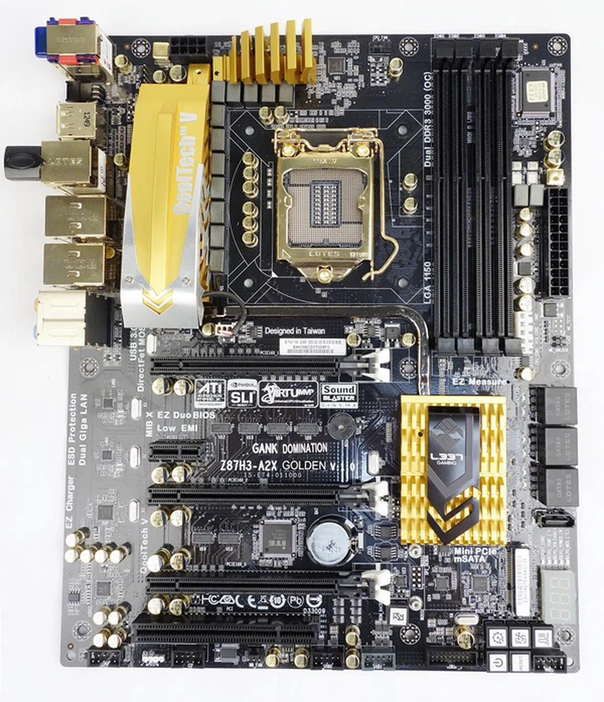
ECS Gank Domination Z87H3-A2X Golden
This board hails from the Gank motherboard series by ECS. It marks the company's effort to capture some market share in the high-end motherboard segment. The ECS Gank Domination Z87H3-A2X Golden is an ATX-sized board with a slew of distinguishing features. For starters, we can see why the board's name has the word "golden" in it. A number of components have been gilded, much like the previous generation ECS Z77H2-AX. However, this is where the similarity ends as the newer ECS board is based on the Intel Z87 chipset, with support for Intel Haswell processors in LGA 1150 packages.

The ECS Gank Domination Z87H3-A2X Golden represents the company's effort to target the high-end market segment for motherboards. We felt that its gilded treatment this time round, has been toned down to lessen the tackiness often associated with opulence.
Like the earlier ASRock counterpart, this ECS board also has a 12-phase power delivery system. Its VRM components are made of "Ice Chokes", dual-cooling MOSFETs, and golden solid capacitors. From the layout, it was rather strange as the typical arrangement of MOSFETs of a contemporary mother is L-shaped, along the two adjacent sides of the CPU socket. However, it appears ECS has decided to cramp a majority of the board's MOSFETs under the larger heatsink that has the words "QoolTech V" emblazoned on it.
Peeking under that very heatsink, we noticed a small fan nested below the larger VRM heatsink. Therefore, it makes sense to do park more MOSFETs under this actively-cooled heatsink.

One of the VRM heatsinks has a hidden secret, a small cooling fan!
This VRM is also connected to the chipset's heatsink by a U-shaped heatpipe. On top of that, the VRM and chipset heatsinks have thermochromic technology that will allow the heatsinks to change their colors based on operating temperatures. This will provide visual cues to the user when the heatsinks become too hot to be handled with bare hands; useful when you've just finished an overclocking run and you need to meddle with the board.

A U-shaped heatpipe connects the heatsink of the board's chipset to the actively-cooled VRM heatsink.
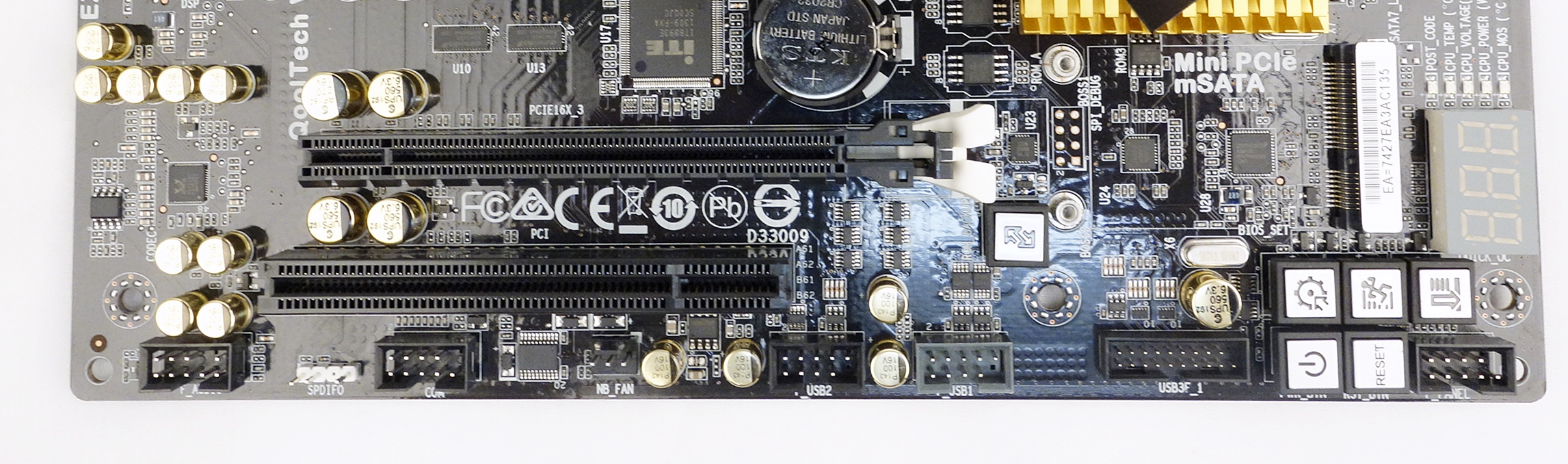
Next, let's take a look at the board's expansion slots. It has three PCIe x16 physical expansion slots and they can be easily identified by their white latches. Depending on how many graphics cards you use with the board, the slot configuration is as follows: x16 or dual x8 or x8/x4/x4. Further to the three main PEG slots, there is a PCIe 2.0 x1 slot, and a legacy PCI slot that stem from the board's Intel Z87 chipset.

There are three PCIe Gen 3.0 x16 slots (with the white latches), one PCIe 2.0 x1 slot and a lone PCI slot.
Beyond the PEG slots, at the bottom edge of the board, we have the usual headers and connector, with a cluster of onboard buttons at the right side. From the left, there is a front panel audio header, a S/PDIF out header, COM port header, a fan connector, a pair of USB 2.0 headers, a USB 3.0 header, and a system panel header.
From the left, there is a front panel audio header, a S/PDIF out header, COM port header, a fan connector for cooling the northbridge, a pair of USB 2.0 headers, a USB 3.0 one, and a system panel header.
The onboard buttons are grouped together, with the exception of the lone ROM backup button that is near the PEG slots. According to the board's manual, activating this button will restore the main BIOS from a backup ROM. This is only necessary when the main BIOS is corrupted.

The ROM backup button.
The other buttons are the the reset and power buttons in a vertical row. The BIOS set button, with the figure of an arrow and a gear, allows you to enter the BIOS utility quickly. The middle button is the Quick OC that allows you to overclock the system. Last of all, the 80P switch controls the information displayed by the debug LEDs. Besides the usual POST error codes, it is capable of displaying the temperature, voltage, and power of the CPU, as well as the MOSFETs' operating temperature. The 80P switch has to be depressed each time to cycle through the information.

Next up, there are five black SATA 6Gbps connectors that are driven by the board's Intel Z87 chipset; four of them are on the right; while the fifth is in vertical orientation (refer to below photo). The remaining pair of SATA 6Gbps connectors are connected to the Asmedia ASM1061 controller, which also drives a pair of eSATA 6Gbps connectors at the rear I/O panel. Due to the controller's ability to drive only two ports, you can't use both sets of ports simultaneously.

The DIMM slots, located to the right of the SATA connector stack, are black, and they support DDR3 memory modules that have been rated for up to 3000MHz.

The board supports overclocked DDR3 memory modules that have been rated up to 3000MHz.
The ECS board has Wi-Fi and Bluetooth modules at its rear I/O panel. There is also a bundled antenna for the wireless module. In addition, there are a pair of RJ-45 ports that allow for "teaming functions." It is the only board to feature eSATA 6Gpbs ports, courtesy of its ASM1061 controller. For its video connectivity options, there is a DisplayPort port, and an HDMI interface. We do find the four USB 3.0 ports a tad lacking as the Intel Z87 chipset supports up to six such ports with a third-party controller (which the ECS doesn't have). Note that there's a clear CMOS button located next to the red USB 2.0/eSATA port.

The rear I/O panel of the ECS board. Some of its unique features include a Bluetooth and Wi-Fi modules that comes with a bundled antenna and dual Gigabit LAN ports.
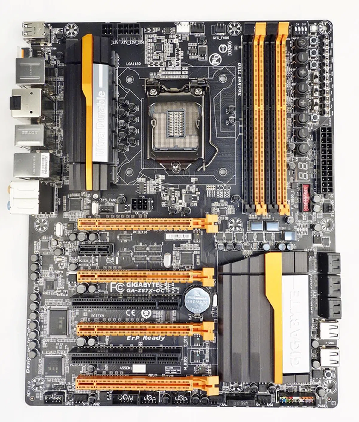
Gigabyte Z87X-OC
The Gigabyte Z87X-OC is a visually striking ATX board from Gigabyte's overclocking series. Splashed with streaks of bright orange in stark contrast against the jet black PCB, the Z87X-OC looks its part as the board also prominently features a number of onboard features that will make it fit perfectly into a open workbench environment of overclockers and power users. We venture to say that this board is built exclusively for unlocked 4th generation Intel Core (Haswell) processors!

The Gigabyte GA-Z87X-OC is an ATX board from the company's overclocking series. Besides its striking color scheme, the board also boasts of a slew of onboard features that will appeal to system builders working in an open workbench environment.
Like high-end boards from Gigabyte, the board features Ultra Durable 5 Plus technology that we first experienced at Computex last year. Thus, the 12-phase power delivery system of the board features voltage regulation module components like the black solid capacitors, which are capable of stable performance even at high operating temperatures. In addition, the board has PowIRstage ICs that are single-package, single-silicon design MOSFETs, which boast of lower operating temperatures, without any concessions on performance.

The Gigabyte Z87X-OC board has a 12-phase power delivery system made up of Ultra Durable 5 components.
True to its overclocking pedigree, and somewhat like the ASRock counterpart, the Z87X-OC has an additional 4-pin 12V (the ASRock Z87 OC Formula has an additional 8-pin 12V connector), on top of the regular 8-pin one. This is to provide additional juice to the CPU during overclocking. Moving south from the LGA 1150 CPU socket, we also see a 6-pin PCIe power connector, this is recommended when two or more graphics cards are installed.

Additional power connectors provide much needed juice for the extreme enthusiasts. For overclocking, the board has an additional 4-pin 12V power connector for the CPU. In the event of installation of two or more graphics cards, there is a 6-pin PCIe power connector handy too.
Speaking of its PEG slots, there are four PCIe x16 physical slots. As there are no PCIe Gen 3.0 PLX switch controllers on board, the Z87X-OC supports up to 2-way SLI for NVIDIA graphics cards. However, for AMD Crossfire configurations, the board is able to support up to 4-way CrossFireX configurations. The first PCIe Gen 3.0 x16 slot is able to run at full speed at x16, if only a single graphics card is installed. In the event of a dual GPU setup, the second card is supposed to be installed in the third PCIe Gen 3.0 x16 slot. Therefore, the standard 16 PCIe 3.0 compliant lanes that's powered by the CPU will be shared between the two installed graphics cards with a x8/x8 bandwidth configuration.

There are four physical x16 slots, only the first three are PCIe Gen 3.0 compliant. The last x16 slot is connected to the board's chipset, operating at x4 PCIe 2.0 speed.
The second PCIe Gen 3.0 slot actually shares bandwidth with the first and third expansion slots. Therefore, in a 3-way PCIe Gen 3.0 compliant graphic setup, the lanes are divided in the following manner, x8/x4/x4. The last x16 slot is only PCIe 2.0 standard, and it is connected to the board's Intel Z87 chipset, running at x4 speed. Do note that only AMD cards are supported in a 4-way CrossFireX configuration. For NVIDIA card owners, they are limited to a 2-way SLI setup. Further to these full PEG slots, the board also has a pair of PCI slots and a lone PCIe 2.0 x 1 slot.
Next, we look at the headers and connectors lining the bottom edge of the board. The headers are made up of front panel audio header, COM port header, a pair of USB 2.0 headers, a USB 3.0 header, and a system panel header with color coding to differentiate between the connectors. Amongst the headers, there are three system fan headers.

The headers are made up of front panel audio header, COM port header, a pair of USB 2.0 headers, a USB 3.0 one, and a system panel header with some form of color coding to differentiate between the connectors. Amongst the headers, there are three system fan headers.
There is a pair of USB 2.0 ports, next to the stack of black SATA 6Gbps connectors. According to the board's manual, the ports are called OC Connect ports. They enable power users to conveniently attach supported devices like flash memory drives to be attached quickly, without having to reach behind when most of the USB ports are located at the rear I/O panel. As you might imagine, this board is engineered for a open test-bench setup rather than to be hidden away within your casing where these and many other features would be harder to utilize.

The pair of OC Connect USB 3.0 ports is used for connecting supported devices in an open workbench environment.
We also uncovered a nugget of information while reading up on the OC Connect ports; apparently, for some unknown reason, only two of the six USB 3.0 ports from the board's Intel Z87 chipset have been utilized. The rest of the USB 3.0 connectivity is handled by two Renesas USB 3.0 hubs, and the hubs drive a total of 6 USB 3.0 ports, found at the rear I/O, and 2 more that are made available with a USB 3.0 internal header. There is the "Clear Battery" button, next to the OC Connect USB 2.0 ports. When pressed, it will have the same affect as removing the battery from the board.

From the top, we can see the "Clear Battery" button that when pressed, it will have the same affect as removing the battery from the board.
The board supports up to 32GB of overclocked DDR3 memory modules that have been rated up to 3000MHz. The area, just below the DIMM slots, is packed with a lot of onboard features for overclocking and tweaking purposes (refer to below photo). Most notable are the set of OC Buttons that will help overclockers adjust their settings in real-time.
And of course, there is a mainstay Dual BIOS switch that allows the board to operate with two sets of BIOSes, and there is even another switch to disable the Dual BIOS feature of the board. Besides good eyesight, prospective users will need to refer to the board's manual for their operational details.

Besides the OC Buttons, there are BIOS switches and a PCIe DIP switch. There is also a row of voltage measurement points that support two methods of measuring voltage, either with a multimeter directly, or attaching the bundled voltage measurement cables to the corresponding points. (Image Source; Gigabyte)
At the rear I/O panel, there is the OC Ignition button that will maintain power to the system's drives and cooling fans, without powering up the CPU. This feature is useful for keeping the cooling fans running to reduce moisture build up during LN2 cooling. It also allows the attached drives to keep operating, and prevent data loss of any virtual RAM drives.

In terms of video ports, there are two HDMI connectors, and a DisplayPort port. There are a total of six USB 3.0 ports, and a pair of USB 2.0 ones. The PS/2 mouse and keyboard port sits on top of a pair of USB 3.0 ports. There are six analog audio jacks, instead of the usual five, as there is an additional jack for side speakers (as such, the S/PDIF connector has been shifted out). In terms of network connectivity, there isn't any wireless modules, but there is a single RJ-45 LAN port.
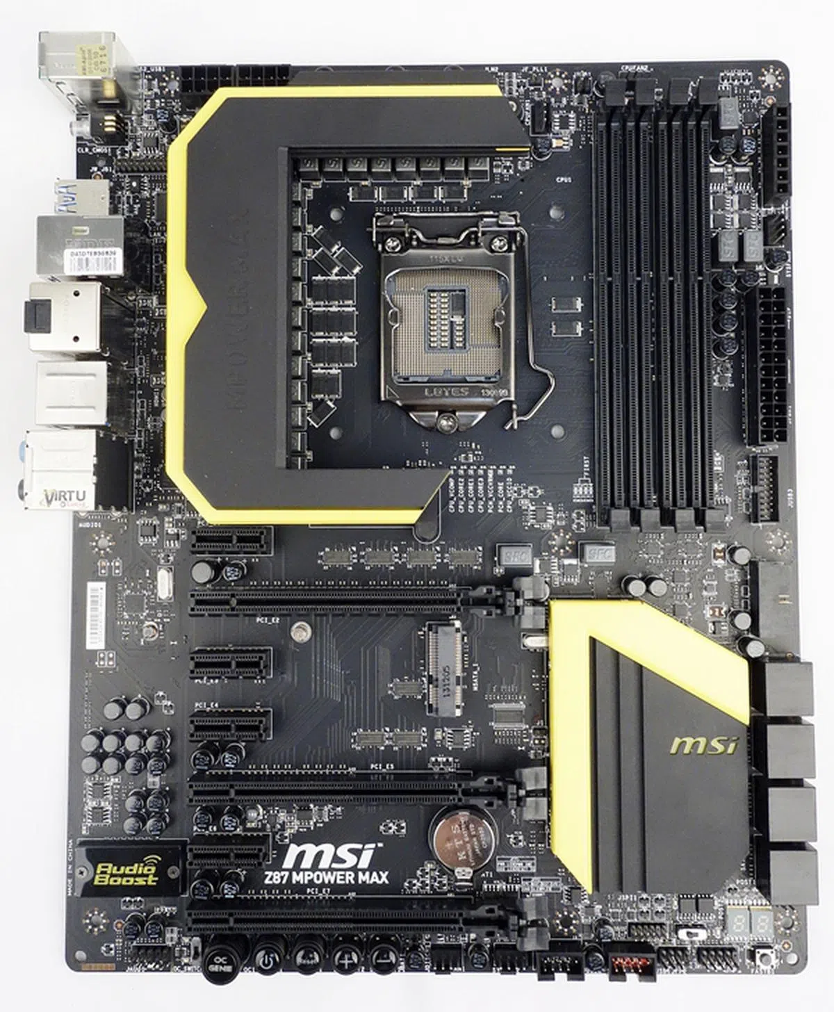
MSI Z87 MPower Max
What struck us about the MSI Z87 MPower Max is how smooth its VRM heatsinks are. Usually, such heatsinks come with sharp and jagged edges, in order to maximise their surface area for optimal heat dissipation. However, this board has overturned this convention, with its smooth finished VRM and chipset heatsinks.

The MSI Z87 MPower Max has a 20-phase power design to ensure the stable power delivery to the CPU and memory of the board. It also features the updated Military Class IV components of its power delivery systems.
From this perspective, we can see two rows of chokes, which are lined up at a right angle, in front of the VRM heatsinks. In terms of its power delivery system, the MSI board has a 20-phase power design to ensure the stable power delivery to the CPU and memory of the board. It also features the updated Military Class IV components of its power delivery systems. They consist of new PowerPak MOSFETs, Hi-c capacitors (Hi-C Cap), super ferrite chokes (SFC), along with solid capacitors (Solid Caps) and Dark capacitors (Dark Caps).

When viewed from the rear, we can see the MSI Superpipe that is essentially an 8mm nickel heatpipe that connects the VRM heatsinks for better heat dissipation.

The MSI Superpipe is embedded in the VRM heatsink. Also notice that while the heatsink is thick, it's grooved internally to increase heat dissipation area.
In terms of expansions slots, the board has three PCIe Gen 3.0 x16 slots, and four PCIe 2.0 x1 slots. With the 4th generation Intel Core Haswell processor being able to only deliver 16 PCIe lanes; hence, on the MSI board, this single PCIe x16 link can be split into two x8 links or three links with a x8/x4/x4 configuration. As a result, the board is able to support up to, either a 2-way NVIDIA SLI setup, or a 3-way AMD CrossFireX configuration. This is also compounded by the fact the MSI board doesn't feature any PLX PCIe Gen 3.0 switches to boost throughput in each PEG slot.

There are three PCIe x16 physical slots, and four PCIe 2.0 x1 slots. We also see a mSATA slot that is sandwiched between the first two x16 slots.
Even as we are looking at the expansion slots of the board, we couldn't help noticing the row of buttons that consists of a triplet of the Easy Button 3 system, and the pair of Direct OC buttons. The Easy Button 3 is made up of the OC Genie, power and reset buttons. The OC Genie button will allow you to overclock the system with just a push of it; while the Direct OC ones, the "+" and "-" buttons, allow for finesse as you can use them to adjust the base clock frequency of the unlocked processor during normal operations of the board.

From the left edge of the board is the front panel audio header. The row of onboard buttons break the succession of the other headers that include a pair for system fans, followed by two USB 2.0 ones. The front panel headers are divided into two sections, with a Go2BIOS button at the end.
To the far right of the bottom edge of the board, there is the front panel audio connector. Next to it is the OC Genie mode switch that provides two overclocking modes for the OC Genie feature. After the buttons, we see two internal fan connectors, and two USB 2.0 headers. Next up, we see two system panel connectors, and to their right, there is a Go2BIOS button that allows you to boot to the BIOS utility without the need for any keyboard inputs. This button is useful as the keyboard is disabled during POST when the "MSI Fast Boot" feature is enabled.
Nearer to the stack of SATA 6Gbps connectors, you'll find more onboard feature such as the usual debug LED segment display, and a multi-BIOS switch that allows for switching between two sets of BIOSes. The two BIOS ROM chips are located at the top of the switch.

The SATA 6Gbps connectors are black, and from the left, the first pair is connected to the board's ASMedia ASM1061 controller, and the remaining six are driven by the Intel Z87 chipset. There is a USB 3.0 header next to the stack of SATA connectors.

Moving to the right, we see the DIMM slots that support overclocked DDR3 RAM modules, rated up to 3000MHz. In addition to the voltage checkpoints that are located near the edge of the board, there is another set of voltage checkpoints near the CPU socket, for monitoring the voltages of the CPU and PCH.

In the vicinity of the DIMM slots, there is the row of voltage point connectors at the edge of the board. Also, near the LGA 1150 CPU socket, there are voltage check points for the CPU and PCH.
The rear I/O panel of the board features a PS/2 combo port, above a pair of USB 2.0 ports. The clear CMOS button has a unique design but it could pose a danger as it may be accidentally pressed. There are a total of six USB 3.0 ports, and its video connectivity options consist of two HDMI connectors (both for outputs), and a DisplayPort port. The S/PDIF out connector sits above the HDMI connector, while the bright canary yellow hue of the RJ-45 Gigabit connector sits atop one of the USB 3.0 stacks.

The clear CMOS button is located next to the PS/2 and pair of USB 2.0 ports, and we would prefer if its design was less outstanding so that the risk of pushing it unnecessarily is reduced.
Motherboard Features Comparison Table
[hwzcompare]
[products=441192,401429,441197,441210,441309]
[width=200]
[caption=Top Intel Z87 Chipset Motherboards Compared]
[showprices=0]
[/hwzcompare]
BIOS Settings
The UEFI BIOS utilities of the boards have their own unique look and feel. In the past, we felt that the GUI-based BIOS was lethargic in terms of responsiveness; however, with this current crop of Intel Z87 boards, it appears that such kinks have been ironed out.
Below, we have highlighted the voltage settings of the boards which we have had to modify during our overclocking efforts to obtain a maximum stable CPU clock speed (since there's little gain from modifying the base clock of the boards). The UEFI BIOS utilities from ASUS and Gigabyte offered the most detailed voltage settings among the compared boards. For the DRAM Timings, we took the default values offered by default settings of each board. We have used a new set of DDR3 memory modules for this round of testing, so do refer to their specifications listed below.
Model | CPUVoltage | DRAMVoltage | Other Voltage Settings |
ASRock Z87 OC Formula
| CPUInput Voltage: Fixed Mode (1.910V) | DRAMEventual Voltage: Auto |
|
ASUS Maximus VIExtreme
| CPU Core Voltage: 1.325000V | DRAM Voltage Frequency: Auto |
|
ECS Gank Domination Z87H3-A2X Golden | CPU Core Voltage: 1.315V | DIMM Voltage: 1.65V |
|
Gigabyte Z87X-OC
| CPU Core Voltage: 1.325V | Profile DDR Voltage: 1.50V |
|
MSI Z87 MPower Max | CPU Core Voltage: Auto | DRAM Voltage: Auto |
|
Test Setup
This is the test configuration for our Intel Z87 motherboard shootout.
- Intel Core i7-4770K (3.5GHz)
- Motherboards:- ASRock Z87 OC Formula, ASUS Maximus VI Extreme, ECS Gank Domination Z87H3-A2X Golden, Gigabyte Z87X-OC, MSI Z87 MPower Max
- 2 x 4GB Crucial Ballistix Elite Series DDR3-1600 (CAS 9-9-9-27)
- MSI GeForce GTX 660 Ti Boost Twin Frozr III OC (GeForce Driver Version 331.65)
- Western Digital Caviar Black 1TB SATA 6Gbps hard drive (one single NTFS partition)
- Windows 7 Ultimate SP1 (64-bit)
Note 1: The price range of the motherboards in the roundup is rather wide. We are focusing on the best options that are locally available from motherboard vendors at the time of evaluation (in December 2013). There are some boards that have additional features like wireless modules or even an OC Panel that is bundled with the ASUS board. Such frills will add on to the costs of each board. But we would be focusing on the overclocking and performance levels of the boards, especially on gaming benchmarks like 3DMark and Tomb Raider.
Note 2: Overclocked settings mentioned above were only used during the overclocking stress test phase. In all other tests, the boards were run at stock performance levels to judge them at level playing field.
Benchmarks
The following benchmarks were used to test the motherboards:
- BAPCo SYSmark 2012 (ver 1.05)
- SPECviewperf 11.0
- Futuremark PCMark 8
- Futuremark 3DMark (2013)
- Tomb Raider
A new addition to our motherboard benchmark suite is Futuremark PCmark 8. It is designed to test the performance of the system on its pre-determined scenarios while tackling a number of content creation applications simultaneously; after which it would generate a general score.
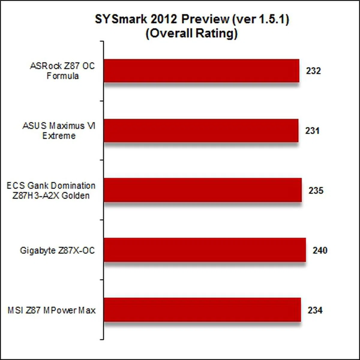
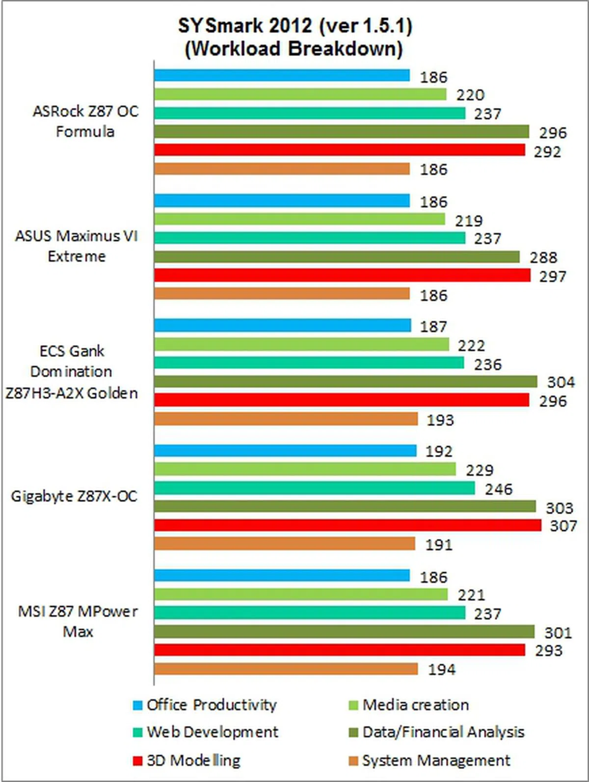
Results - SYSmark 2012
SYSmark 2012 is the first of our synthetic benchmarks and we have updated it to version 1.5.1. Its test scenarios have changed since the update, and they consist of Office Productivity, Web Development, Media Creation, Data/Financial Analysis, 3D Modeling, and System Management. The board that pulled ahead was the Gigabyte Z87X-OC, with the ECS Gank Domination Z87H3-A2X Golden, and MSI Z87 MPower Max trailing in that order. For the trio, it was their scores in 3D Modeling and Data/Financial Analysis tests, which enabled them to surge ahead of the rest of the motherboards.
 |  |
Results - SPECviewperf 11.0
The Gigabyte board clinched the top spot for the SPECviewperf 11.0 benchmark software suite which is known to stress the graphics and memory subsystems.

Results - Futuremark PCMark 8
For this synthetic benchmark, we expected the winning trio from the SYSmark 2012 tests to show their mettle here. Instead, the ASRock board managed to displace ECS board; hence, the three boards that pulled ahead are the Gigabyte Z87X-OC, with the ASRock Z87 OC Formula, and MSI Z87 MPower Max respectively.

Results - Futuremark 3DMark (2013) & Tomb Raider

For the two gaming benchmarks, it was the ASUS Maximus VI Extreme that stood out given the similar graphics subsystem across the comparison. It managed to churn out the highest average frame rates during our Tomb Raider tests; while for the 3DMark 2013 test scenarios, it showed strong and consistent performance when peering at the detailed test rundown. The Gigabyte board however got the highest overall score in 3DMark 201, but it wasn't ahead of the ASUS board by much.
Temperature
Despite its VRM heatsink with active cooling, the ECS board had the highest operating temperature of 43 degrees Celsius recorded. Even its chipset heatsink recorded a high of 45 degrees Celsius. In addition, the Gigabyte board was the other one whose VRM temperature, under load, was above 40 degrees Celsius. The other boards' recorded VRM temperatures were below 40 degrees Celsius, with an average value of 34.6 degrees Celsius. MSI's Z87 MPower Max was among the coolest operating boards under load, along with ASRock Z87 OC Formula.

Power Consumption
MSI turned out to have the lowest power draw during idle and load operations, followed by the Gigabyte board. ASUS with its truckload of features and ICs enabling the extra functions naturally consumed a little more power than the rest of the boards.

Overclocking
In our attempts to overclock the current Intel Z87 boards, we set the CPU base clock at 100MHz (for obvious reasons that it's pretty much futile to mess with this base clock), and adjusted their CPU Core Ratios accordingly to achieve the best possible CPU overclock. At the same time, we also tweaked the different voltage CPU and DRAM settings in order to achieve a stable overclocked state as listed out on the test setup page.
Model | Maximum CPU Core Ratio Achieved
| Maximum Overclock Achieved |
ASRock Z87 OC Formula | 45 | 4.5GHz |
ASUS Maximus VI Extreme | 48 | 4.8GHz |
ECS Gank Domination Z87H3-A2X Golden | 43 | 4.3GHz |
Gigabyte Z87X-OC | 47 | 4.7GHz |
MSI Z87 MPower Max | 46 | 4.6GHz |
To ensure the clock speeds weren't just for show, we used Cinebench 11.5 scores to determine the gains from overclocking, and it was the ASUS Maximus VI Extreme that led the pack with its almost 30% performance boost!

Conclusion
From what we've encountered and since the Intel Z87 chipset is a high-end platform for the Intel Haswell processors, we can safely conclude that this current crop of motherboards are in line with our expectations. The boards do boast of high-end features that will appeal to the varied needs of the very group of specialized users. The wares from the board manufacturers boast of good build components, with each attempting hard to differentiate its offerings in this crowded market segment. Therefore, we have taken their unique features into consideration as we tabulated their scores below. The performance scores take into account each board's stock performance, overclocking capabilities, temperature and power performance, and they have been adjusted accordingly.
Model | Features | Performance | Overall | Suggested Retail Price |
ASRock Z87 OC Formula | 8.0 | 7.5 | 8.0 | S$468 |
ASUS Maximus VI Extreme | 9.5 | 8.0 | 8.5 | S$609 |
ECS Gank Domination Z87H3-A2X Golden | 7.5 | 7.0 | 7.5 | S$450 |
Gigabyte Z87X-OC | 8.0 | 8.0 | 8.0 | S$422 |
MSI Z87 MPower Max | 7.5 | 8.0 | 8.0 | S$452 |
The ASUS Maximus VI Extreme board’s performance is stellar where it counts, namely in overclocking and gaming benchmarks. Its overclocking performance is helped by ASUS’ proprietary DIGI+ PWM systems and the on-board energy-saving EPU chip to allow for precise voltage control.
The ASUS Maximus VI Extreme board’s performance is stellar where it counts, namely in overclocking and gaming benchmarks. Its overclocking performance is helped by ASUS’ proprietary DIGI+ PWM systems and the on-board energy-saving EPU chip to allow for precise voltage control. In line with its ROG heritage, the inclusion of a high-speed PLX PEX8747 splitter chip allows gamers to set up a multi-GPU configuration for their extreme gaming requirements. For power users, the OC Panel offers convenience in overclocking and system monitoring. Another bundle of surprise is a mPCIe Combo II expansion card. This card allows for the installation of M.2 (NGFF) SSD so that users can take advantage of Intel SRT (Smart Response Technology -- Intel's hybrid SSD caching solution) or otherwise from its enhanced interface. In addition, the expansion card houses a dual-band IEEE 802.1ac Wi-Fi and Bluetooth v4.0 module. A removable ASUS 2T2R dual band Wi-Fi moving antenna completes the whole package. The board is priced at an exorbitant price of S$609; however, given the board’s rich feature set, excellent overclocking experience and top-end performance, it truly deserves the top accolade for our shootout.
The Gigabyte Z87X-OC is a high-end board that turned in consistently high performance scores during our stock testing. The board is targeted at users who want to overclock their Intel Z87-based system without worrying about performance stability issues. To reiterate, the board boasts of Ultra Durable 5 Plus components. In particular, the board features specially designed MOSFETs called PowIRstage ICs. They are touted to have lower operating temperatures while maintaining top performance, which we found to be true. Gigabyte fans would be pleased to know that the DualBIOS feature of the board has been widely copied by other manufacturers under different guises. This nifty feature will allow power users to keep one set of BIOS for their overclocking needs, and another set for regular operation. Another strong suit for this board is the full complement of features that enable using the board for advanced overclocking needs in an open test-bench environment outside of the casing - it has the most number of controls and features for such use of any other motherboards we've seen to-date. Wireless connectivity would have really rounded up the overall package, but that would have added to the board's cost. As it stands now, with an attractive price point of S$422, it takes our Value For Money Award for a board that excels on core performance and features.
The MSI Z87 MPower Max features Military Class IV components that make up its power delivery system. The Hi-c capacitors, with super ferrite chokes and dark capacitors ensure its overclocking capabilities. In fact, the board has been OC Certified by the company as a sign of confidence about its said abilities. Other features targeted at overclockers include its voltage read-out points to an easy on-board OC button for easy overclocking. For ease of configuration, as well as for back up purposes, the board’s Multi-BIOS II feature allows users to store different settings in each of its two set of BIOSes. The on-board buttons like the Easy Button 3 and Direct OC are a boon to power users. The OC Genie allows the system to be overclocked with the push of a single button. For the more ardent overclocker, the pair of Direct OC buttons will allow for modification of the CPU ratio and base clock frequency in the operating system environment. The board has an interesting add-on card in the form of a Wi-Fi and Bluetooth module that supports Intel Wireless Display (WiDi) technology. On top of the usual wireless connectivity options of IEEE 802.11 a/b/g/n and Bluetooth v 4.0, this module allows you to stream HD content from your system to an Intel WiDi-enabled display or projector. It's a decent all-rounder and comes as a close recommendation to the Gigabyte Z87X-OC if you prefer MSI's overall proposition better.
The ASRock Z87 OC Formula has one of the more unique features such as a waterproof PCB that will appeal to power users who are into liquid cooling. Rig builders who are afraid of leakage from their liquid cooling systems may also apply. Another notable feature is the Purity Sound technology that features an on-board Realtek ALC1150 audio codec, complete with EMI shielding to minimize distortion due to electrical interference. Together with the accompanying TI NE 5532 amplifiers, this on-board audio system is touted to provide high quality aural experience. So while its features might be unique, overall performance was average, though the board does have a decent showing in some of the tests. Take note that it's an EATX board, so checking on casing compatibility is a must.
One of the key features of the ECS Gank Domination Z87H3-A2X Golden is its Durathon standard components. They are of high-quality build and have been subjected to stringent testing conditions. In particular, the board’s “super solid” capacitors are claimed to have a lifespan of 22 years, which is about seven times longer than average ones. These capacitors can operate at extreme temperatures, up to 100 degrees Celsius. To add to its durability, the board’s PCB has weaved glass fabric to guard against warping under humidity and high temperatures. Unfortunately, its performance leaves much to be desired for a board of this caliber. While it's not all bad, it's not outstanding in any manner. Low points are its temperature and overclocking prowess that are important factors for this pedigree of boards.
 | |
 | |
 |  |
 | |
 |  |


Our articles may contain affiliate links. If you buy through these links, we may earn a small commission.